Introduction

This documentation describes and explains the Quantum Key Distribution system developped by VeriQloud. This documentation is still under construction.
Here is a datasheet of the system.
The source code can be found in the following repos
- kiwi_pcb (printed circuit boards)
- kiwi_fpga (fpga source code)
- kiwi_hw_control (hardware control software; deployment; monitoring)
The above repos together with this documentation make up the hardware of the system. That should get you up to the raw key.
Software on top of that, such as post processing, key management, QKD and non-QKD based applications can be made available on an individual basis. Please contact us directly.
PM-QKD
Prepare and Measure protocol (PM-QKD) includes a QKD transmitter party Alice and a QKD receiver party Bob. Alice prepares and sends quantum states to Bob through a quantum channel. Bob measures the quantum states. The result (after post-processing) is a common final key available to Alice and Bob.

Time bin encoding

Alice uses a continuous wave laser, cuts out two pulses with an amplitude modulator and applies a differential phase to the two pulses. One of four phases is choosen randomly in BB84 fashion. Bob also applies a random phase, interferes the pulses using an umbalanced Mach-Zehnder interferometer and measures them on single-photon detector. More details are provided in the optics section.
For decoy state QKD the amplitude of the double pulse is chosen randomly from a small set.
Our technological approach
We adopt a modular design. The heart of the system is the VQ Card performing real time digital processing and analog control. This card together with the computer, some electronics and the optics is in a rack mountable enclosure. The classical network and clock distribution is external and must be provided for the system. The laser and detector are inside the encosure by default but can be made external for flexibility. This way, development teams can use their own laser or detector to best suit their project. The protocol we run on the system is standard BB84 with time-bin encoding. Other protocols can be implemented but might require modifications of the FPGA code and other components. The computer we use is a fairly powerful standard PC to leave room for custom postprocessing applications.

Our network philosophy is to separate the quantum and the classical network. The classical communication can happen over any ethernet connection. The reason behind this choice is that routing on the quantum network must be done with minimal optical losses. Coprapagation of the classical and the quantum signal on the same network inevitably increases the losses as well as the complexity. Nevertheless, shared networks are possible with proper filter designs. However, they depend strongly on the topologies and requirements of the operator. Such setups have not been tested with this system yet.

This is an overview of the logical levels. This architecture involves four layers (the physical hardware layer (PHY), the QKD Network Layer (here called Node), the key management service layer (KMS), the application layer (APP). Each layer can be modified independently of the other ones for more flexibility.
- The application layer consists of user devices and applications, which make key requests to the Key Management Service (KMS) layer. These devices and applications use these keys to encrypt data in a secure way.
- The KMS layer obtains keys from the quantum network layer and distributes the keys to their designated hosts in the application layer. The KMS layer must ensure the integrity and confidentiality of the keys.
- The Quantum Network Layer: executes all the post-processing steps on the keys produced from the physical layer to get final secure keys. It coordinates key routing between nodes and provides the keys directly to the KMS layer. The Veriqloud software doing these tasks is called Node.
- The physical hardware layer (PHY) consists of the quantum channel and physical QKD hardware devices. These devices are responsable for generating the keys. After a key is produced, it is passed to Node where it is processed as described above. The PHY layer and Node share data through PCIe.
We make the physical hardware layer as well as Node open source. The KMS and applications remain closed source.
Post processing
For the BB84 protocol without decoy states, there are three steps to process the raw key into the final key:
- Sifting: the basis choice for each detection event is compared between Alice and Bob and the non-matching events are discarded.
- Error correction: mismatched bits are corrected using parity checks (via a low-density parity check code).
- Privacy amplification: the key is compressed to compensate information leakage (via Toeplitz hashing). The number of bits leaked in error correction is exactly known. The number of bits leaked to Eve on the quantum channel can be estimated by \( h(\textrm{qber}) \), where \(h\) is the binary entropy function. The qber here is the measured qber plus a few standard deviations to account for finite size statistics.
Classical network and external clock
The system requires two external clocks, 10MHz and 1PPS (pulse per second). The stability between Alice and Bob should be around 100ps on a timescales of around 100us. This is to ensure Bob can measure the pulses with a 100ps precision. Absolute timing stability is not important.
The system also requires a standard ethernet network (e.g. 1Gbit/s) for low-level communication and post processing.
We use the White Rabbit Switch to do both over a single optical channel.
Optics
Alice
 We use an external Laser: Thorlabs SFL1550P. Butterfly package, fully controlled by Laser Driver.
We have the following components on Alice's box:
We use an external Laser: Thorlabs SFL1550P. Butterfly package, fully controlled by Laser Driver.
We have the following components on Alice's box:
- Amplitude Modulator iXblue MXER-LN-10-PD-P-P-FA-FA-30dB
- Phase Modulator iXblue MPZ-LN-10-P-P-FA-FA
- Filter from AMS OZ Optics custom band pass;
- passband: 1510nm - 1585nm
- transmission: 0.72dB @ 1550nm
- rejection: 61dB @ 850nm, 30dB specified elsewere
- Variable Attenuator: Voltage-controlled Attenuator on Dark Mode fs.com
- Manual Attenuator: Manual Attenuator Thorlabs VOA50
Bob
 We have the following components on Bob's box:
- Filter from AMS OZ Optics custom band pass;
- passband: 1510nm - 1585nm
- transmission: 0.72dB @ 1550nm
- rejection: 61dB @ 850nm, 30dB specified elsewere
- Polarization modulator from AMS LUNA (General Photonics). After Polarization Modulator all fibers are polarization maintaining ones P3-1550PMY-1.
- In Line Fiber Polarizer from Thorlabs
- Phase Modulator iXblue MPZ-LN-10-P-P-FA-FA
- Interferometer. Fully passive with two Polarization maintaining beam splitters PN1550R5A2 (BS) + one Polarized Beam Splitter (PBS) + 2m Polarization maintaining fiber PMP-15-R-L-2-2SA-2SA + 1m Polarization maintaining fiber PMP-15-R-L-1-2SA-2FA. All ends for all BS and PBS used for the interferometer are with the narrow key of each connector aligned to the slow axis of the fiber. Only 2m Polarization maintaining fiber has the narrow key of one connector aligned to the fast axis of the fiber (the one connected to the input of PBS)

For detection, we use an external Avalanche Photo Diode OEM module by Aurea (standard grade) with datasheet.
Drivers and amplifiers
-
Laser driver: Koheron CTL300E
- Communication over serial from FPGA.
- 6V-33V power.
-
Amplifier for Amplitude Modulator: ZX60-4016E-S+, pdf datasheet.
- Power: 12V 400mA.
- Vamp 0V-0.9V to control the gain.
- 21dB gain, 8Vpp output max.
- SMA in/out.
-
Amplifer for Phase Modulator of Alice: ZHL-2X-S+, pdf datasheet.
- Power: 24V 600mA
- 20dB gain, 17.8Vpp max
- SMA in/out
-
Amplifer for Phase Modulator of Bob: ZHL-32A-S+, pdf datasheet.
- Power: 24V 600mA
- 25dB gain, 17.8Vpp max
- SMA in/out
-
Pulse generator: Highland Technologies J240
- Power: 12V
- 140ps FWHM pulse, 0V-0.75V pulse amplitude
- Adjustable trigger level
Electronics
As reminder, here is the logical overview of the system
The physical layer (PHY) is in charge of generating the raw keys, which are then passed to Node. The PHY layer includes:
- Physical hardware
- Device driver and Control API
Physical hardware

This is an overview of the physical hardware. There are 2 groups of components:
- Optics and their drivers: Laser, Laser Driver, Pulse Generator, Amplifiers, Single Photon Detector, other optical components. The detail of each components and physical connections are explained in Optics chapter
- Electronics: White Rabbit Switch (WRS), Power Supply system, digital to analog converters (DA) and other electronics components.
The picture below shows the system of electronics, electrical power supply and interface with Optics.

Some abbreviations: Pulse Generator (PG), Amplitude Modulator (AM), Single Photon Detector (SPD), true Randon Number Generator (tRNG), Personal Computer (PC), Time to Digital Converter (TDC), Digital to Analog Converter (DAC)
Device driver and Control API
To complete the PHY layer, it requires a software layer to control the physical hardware. It includes:
- Device driver: this is the low-level software handles PCIe communication (using XDMA) between PC and FPGA. It operates at OS kernel level and is written by AMD (Xilinx)
- Control API: this is the high-level software that runs at user level to configure and control the FPGA via the device driver. The user sends commands and data to FPGA from this API
Instructions to install the driver and source code of Control API is available in kiwi_hw_control github repos. Os level documentation is also provided in the User Guide section.
Sub-Chapters
- PCB board design: describes the Motherboard Bread70, Power Supply Distributors, ATX, Power Meters, and future PCB designs
- FPGA programming: describes logic design in FPGA and corresponding Control API
- WRS, Computer, tRNG: details of these components
Design PCB
In this section, we will describe the PCB design for the power interface and Kiwi MB, as well as the specific functionalities implemented on these boards, their role, and their integration into the overall system.
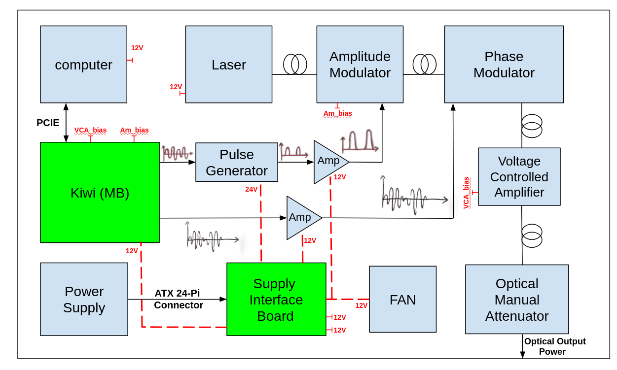
I. Supply Interface Board
The Supply Interface Board acts as an interface between the main power supply and the electronic, optical, and computer components, as shown in the figure below.
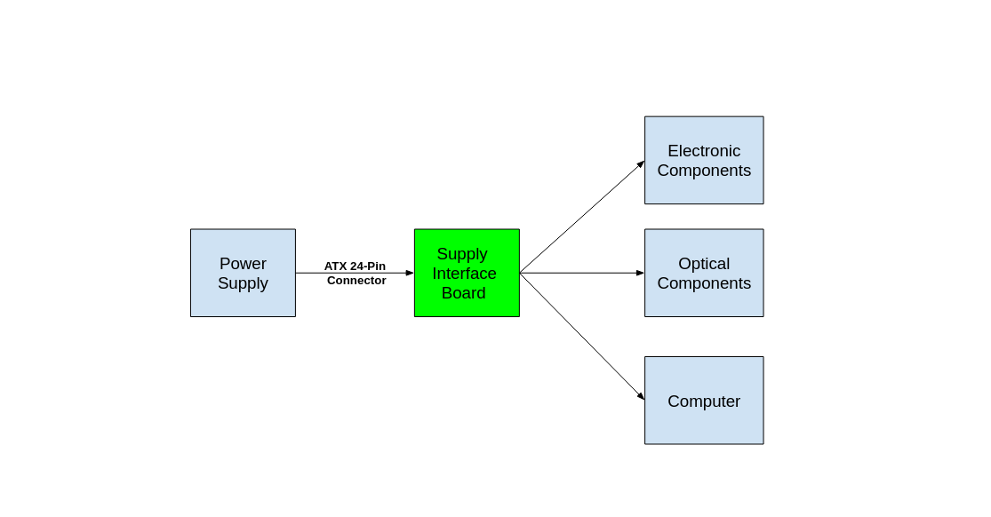
Spécifications:
Outputs:
- 6 × 12 V (total 24 A),
- 1 × 5 V/1 A,
- 1 × ±12 V (total 1.2 A/0.1 A),
- 1 × 24 V/0.6 A.
Main Power Supply:
- Powered by a PC ATX power supply connected via a 24-pin ATX connector.
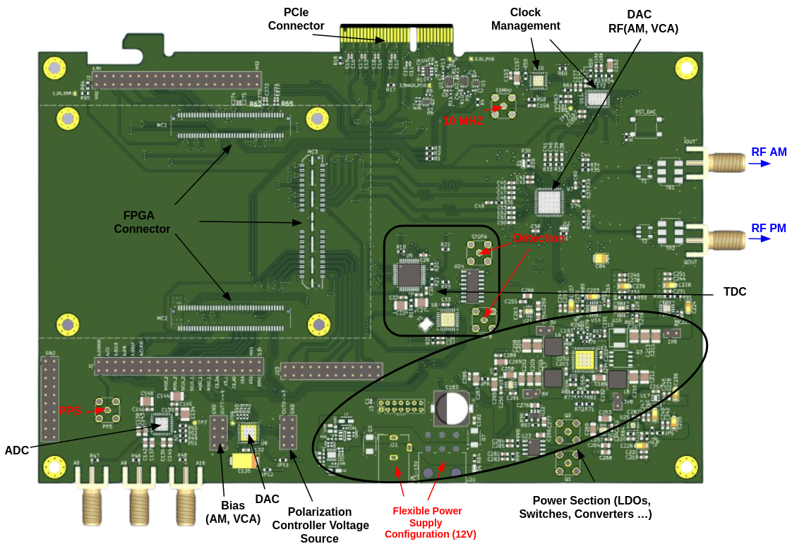
II. Kiwi_MB
The Kiwi Motherboard (Kiwi_MB) is designed for the management and processing of analog and digital signals. It features a slot for the XEM8310 FPGA from OpalKelly, a PCIe connector for interfacing with the computer, as well as a section dedicated to clock and power management. The board also includes DACs and ADCs with SMA inputs and outputs for signal processing.
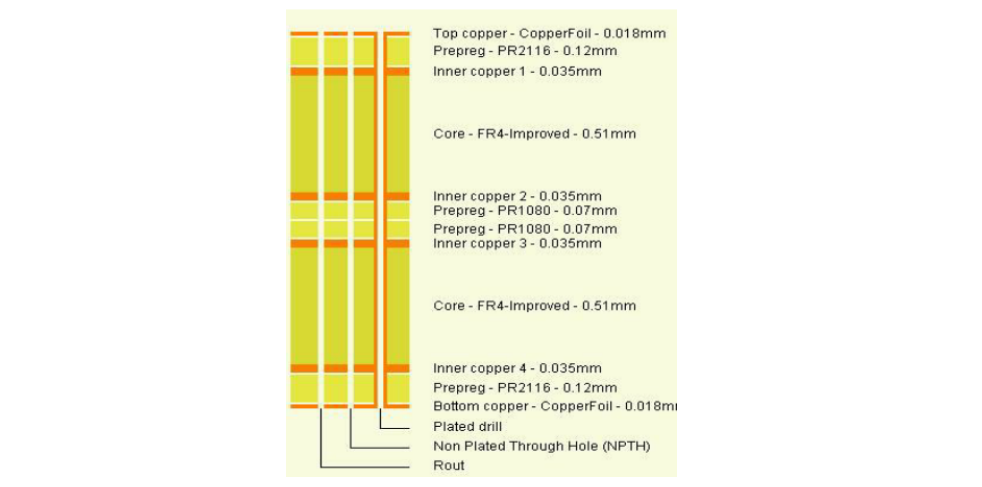
Materials and Stack-up
| Category | Détails |
|---|---|
| Dimensions | Width: 200.0 mm, Height: 138.4 mm |
| Number of layers | 6 (see the figure below) |
| Board thickness | 1.55 mm |
| Base material | IS400 (Tg: 145-150°C) |
| Copper | Outer layer: 18μm, Inner layer: 35μm |
| Minimum hole size | 0.45 mm |
| Trace design | All traces are designed to ensure optimal adaptation to signal frequencies and power, maintaining a characteristic impedance of 50 ohms. |
Functionalities Implemented on Kiwi_MB PCB:
Power Management:
The Kiwi Motherboard (Kiwi MB) is powered by a 12 V supply, which is then converted into multiple voltages through the following Power Management system:
- Five Buck Converters: Producing 1.8 V, 3.8 V, 3 V, 6 V, and 10.5 V.
- One Buck-Boost Converter: Generating an inverted -10.5 V.
- The system includes twelve jumpers: four standard connectors and eight 0 Ω resistors, which must be installed one at a time, verifying the voltages at each step.
- Finally, 8 Linear Regulators (LDO) provide additional voltages: 3.3 V (x2), 2.5 V, 3.8 V, 5 V, and 1.2 V (x3), ensuring stable power for the components.
Clock Management:
The clock management architecture aims to manage synchronization signals in order to improve the system's precision. A 10 MHz reference signal from the White Rabbit Switch (WRS) is sent to the CDCLVD2104, a clock signal buffer, which then passes it to the LTC6951 to generate the necessary clocks for the AD9152 fast DACs, as well as for the TDC and TTL Gate via the FPGA. The CDCLVD2104 also generates the 10 MHz SPI synchronization signal. Additionally, the PPS (Pulse Per Second) signal from the WRS is used as a reference signal for clock alignment, ensuring precise synchronization of the system's components.
DACs and ADCs:
Kiwi_MB contains two DACs and one ADC for signal conversion and generation:
- DAC81408RHAT: This DAC is used to generate polarization voltage signals (AM and VCA) on channels 6 and 7, as well as for the polarization controller on channels 0 to 3.
- AD9152 Fast DAC: A high-speed DAC used to generate the RF signals RF_AM and RF_PM, necessary for producing analog RF outputs sent to the amplitude and phase modulators.
- AD7175-8 ADC: An analog-to-digital converter with three inputs for converting analog RF signals into digital format for further processing.
- These components are managed by the FPGA to ensure efficient signal conversion and the generation of the necessary voltages for the different channels.
TDC:
The TDC system uses four components to convert the arrival times of qubits into digital data. The single-photon detector generates raw data, which is retrieved via an SMA connector and sent to the DS90C031B, an LVDS driver, and then transmitted to the AS6501. The AS6501, a Time-to-Digital Converter (TDC), measures the arrival times and converts them into digital data. The reference signal, generated by the ECX-32 crystal and the Si55319, synchronizes the entire system by producing a differential signal sent to the AS6501, ensuring precise time measurements.
Integration of the Kiwi_MB and Supply Interface Board in the Kiwi Box
Below is a diagram illustrating an example of the integration of the Kiwi_MB and the power interface board, as well as their interaction with the electronic and optical components in Alice's box.
FPGA module introduction
The FPGA integration module XEM8310-AU25P is a product of opalkelly, using AMD Artix UltraScale+ FPGA. All information about XEM8310 is available on Documentation portal of opalkelly. From website you can also download:
- FrontPanel to setting devices, loading bitstream, flash,...
- Vivado board file
- Pins list
This FPGA module will be plugged to the "Bread70" PCB to communicate with all ICs on board.
Vivado project
The RTL source code and Vivado block design is available on GitHub kiwi_fpga. Follow the instructions in README to rebuild Vivado project and block design from Tcl script. Then you have fully access to the project and can generate the bitstream for FPGA on your local machine.
The main blocks in project:
- XDMA
- Clock and reset
- Fastdac
- TDC
- DDR4
- TTL gate
- Decoy signal
- SPI
- ILA debug
Reading the detail of each block in sub-chapters
Prepare FPGA board
Configuration VIO voltage for XEM8310 is the first step to do after getting FPGA. Simply download the FrontPanel API from opalkelly website to your local machine, connect the USB-C and change these VIO settings:
- VIO1 = 1.8V
- VIO2 = 2.5V
- VIO3 = 3.3V
Restart the FPGA module and verify the VIOs. Then you can plug FPGA module to power verified Bread70.
Loading bitstream
There are 2 ways to load bitstream to FPGA
- USB and FrontPanel API: Install FrontPanel API and Configure Device with your bitstream
- JTAG: Simply Open Vivado Hardware manager, Open target and Program device
You can only have access to ILA debug windows in Vivado by JTAG. With this solution, you also can check the Calibration Process of DDR4. I tested severals FPGA modules with the same bitstream, some of them pass the Calibration Process smoothly, some don't.
Flashing bitstream
Using JTAG
Specification
There are 2 non-volatile memory to flash board XEM8310. Read Specification of the board
- System Flash
- FPGA Flash
We are going to choose FPGA Flash mode, using 32MiB QSPI non-volatile memory Opalkelly Flash Memory
Generate specific bitstream
Usually, you generate bitstream in vivado -> top.bit configuration file To be able to load .bit configuration to Flash Memory. Add these to .xdc constraint
set_property BITSTREAM.CONFIG.EXTMASTERCCLK_EN disable [current_design]
set_property CONFIG_MODE SPIx4 [current_design]
set_property BITSTREAM.CONFIG.SPI_BUSWIDTH 4 [current_design]
set_property BITSTREAM.CONFIG.SPI_FALL_EDGE YES [current_design]
set_property BITSTREAM.CONFIG.CONFIGRATE 85.0 [current_design]
Generate bitstream with these added constraints -> top.bit. This bit file only can be used by load it to FPGA Flash
Create the memory configuration .mcs file
In vivado: Tools -> Generate Memory Configuration File -> Choose...
- Format: MCS
- Memory Part: IS25WP256D-x1x2x4
- Filename:/PATH_TO/top.mcs
- Interface:SPIx4
- Load bitstream files: /PATH_TO/top.bit
- Start Add at 0, direction up
Click OK to generate top.mcs
Load the memory configuration file
In vivado:
- Open Hardware Manager
- Right click on Target -> configuration Memory Device
- choose the Memory part, top.mcs
- Choose: Erase, Program, Verify
- Program -> Wait it to finish
Power cycle
Turn off and turn on FPGA. The bitstream should be loaded after 2-3s. Ready to check
Using FrontPanel
Generate the specific bitstream as Using JTAG method
Download and install FrontPanel
run:
sudo ./install
build flashloader
cd Samples/FlashLoader/Cxx/
sudo make
Download the Samples for XEM8310
- Download from opakelly Files Download
- copy the flashloader.bit to ../Samples/Flashloader/Cxx/
Load bitstream
Create a bash script to flash your specific bitstream in /PATH_TO_BIT/
#!/bin/bash
pushd FrontPanel-Ubuntu22.04LTS-x64-5.3.6/Samples/FlashLoader/Cxx/ || exit 1
flashloader w /PATH_TO_BIT/Bob_top_wrapper.bit
popd
Power cycle the board and check
XDMA
XDMA block use "DMA for PCI Express (PCIe) Subsystem" IP supported by AMD. You can click the IP in block design to see the configuration parameters. For Kiwi device:
- Use 4 lanes at full speed 8GT/s
- Axilite 32 bits
- Axilite master space 32MB
- Axistream 128 bits, clock 250MHz
- Use full 4 axistream channels (H2C/C2H)
The picture below shows the actual number of channel and purpose of each channel

From Axil of XDMA, connect with AXI Interconnect IP to divide address space for sub-modules. Changing the size of address space depends on the number of registers need to be written through Axil to Axil of sub-modules. You can check the Axil address distribution in block design or in the table below:
| Offset | Range | Target RTL module/ IP |
|---|---|---|
| 0x0000_0000 | 0x0000_1000 4K | tdc/tdc_mngt/TDC_REG_MNGT_v1_0.v |
| 0x0000_1000 | 0x0000_1000 4K | ddr4/ddr_data_reg_mngt.v |
| 0x0001_0000 | 0x0000_1000 4K | fastdac/jesd204b_tx_wrapper.v |
| 0x0001_2000 | 0x0000_1000 4K | clk_rst/clk_rst_mngt.v |
| 0x0001_3000 | 0x0000_1000 4K | tdc/time_spi/axi_quad_spi |
| 0x0001_5000 | 0x0000_1000 4K | ttl_gate_apd.v |
| 0x0001_6000 | 0x0000_1000 4K | decoy.v |
| 0x0002_0000 | 0x0001_0000 8K | spi_dacs_ltc/axi_quad_spi |
| 0x0003_0000 | 0x0008_0000 64K | fastdac/jesd_transport.v |
Clock and reset management
Clock tree
This is an overview of the clock distribution for Kiwi device. There are 3 clock sources:
- Source 100 MHz for PCIe comes from mother board of PC
- Source 100 MHz for DDR4 comes from oscilator on XEM8310 modules
- Source 10 MHz and PPS comes from White Rabbit Switch(WRS)
WRS 10 MHz is reference for PLL LTC6951 to generate clock pairs (sysref 3.125 MHz and refclk 200 MHz) for Fast DAC AD9152 and FPGA. PLL LTC6951 requires a SYNC signal to align all outputs to input, I use WRS PPS and 10 MHz to generate this signal, then the outputs will be aligned to PPS.
reflck 200 MHz is is the source clock for all logics in fpga, PPS is reference for synchronization

Module RTL
Purpose of this module:
- Manage the input clocks
- Generate the resets for other RTL modules
- Generate SYNC signal for clockchip on board Bread70

Port descriptions
| Signals name | Interface | Dir | Init status | Description |
|---|---|---|---|---|
| fastdac_refclki_p/n | cr_ext_cr | I | 200MHz | input of jesd refclk from clockchip |
| fastdac_sysref_p/n | cr_ext_cr | I | 3.125MHz | input of jesd sysref from clockchip |
| fastdac_syncout_p/n | cr_ext_cr | I | - | input of jesd syncout from receiver |
| ext_clk10_p/n | cr_ext_cr | I | 10MHz | input of 10MHz from WRS |
| ext_clk100_p/n | cr_ext_cr | I | 100MHz | input of 100MHz from clockchip |
| axil signals | s_axil | IO | - | standard axilite interface for r/w registers |
| s_axil_aclk | Clock | I | 15MHz | clock for axil interface |
| sys_reset_n | Reset | I | - | system reset, active LOW |
| clk_ddr_axi_i | Clock | I | 300MHz | clock to generated from MMCM of DDR4 |
| rst_ddr_axi_i | Reset | I | - | reset synced to clk_ddr_axi_i |
| fastdac_gt_powergood_i | - | I | - | powergood indicator of jesd204B core |
| pps_i | - | I | - | PPS from WRS |
| lclk_i | Clock | I | - | lclk domain of tdc module |
| rstn_axil_o | Reset | O | - | Reset axil interface in others modules |
| rstn_ddr_axi_o | Reset | O | - | Reset AXI interface of DDR4 |
| fastdac_refclk_o | Clock | O | 200MHz | Refclk for QPLL in JESD204_PHY IP |
| fastdac_coreclk_o | Clock | O | 200MHz | Clock for logic in 200MHz domain |
| fastdac_corerst_o | Reset | O | - | Reset for fastdac core |
| fastdac_sysref_o | Clock | O | 3.125MHz | Sysref for jesd204b core |
| fastdac_syncout_o | - | O | - | syncout for jesd204b core |
| clk10_o | Clock | O | 10MHz | clk10 SE (single-ended) |
| clk100_o | Clock | O | 100MHz | clk100 SE |
| sync_ltc_o | Clock | O | 2ms HIGH | SYNC signal for clockchip output alignment |
| tdc_rst_o | Reset | O | - | Reset for tdc clock reset module |
| lrst_o | Reset | O | - | Reset for tdc module in lclk domain |
| ttl_rst | Reset | O | - | Reset for ttl_gate module |
| decoy_rst | Reset | O | - | Reset for decoy module |
| gc_rst_o | Reset | O | - | Reset for tdc module in clk200 domain |
| ddr_data_rstn_o | Reset | O | - | Reset for ddr_data module |
User parameters
| Parameter | Value | Description |
|---|---|---|
| C_S_Axil_Addr_Width | 10 | Address width of axil interface |
| C_S_Axil_Data_Width | 32 | Address width of axil interface |
Axilite registers:
- Base Address: 0x0001_2000
- Offset address slv_reg(n) : 4*n
slv_reg0 - R/W Access - Trigger Control
| Bits | Signal name | HW Wire | Action/Value | Description |
|---|---|---|---|---|
| 31:2 | - | - | - | Reserved 0 |
| 1 | clockchip_sync_o | clockchip_sync | Pull LOW to HIGH | Send trigger to generate SYNC signal for external clockchip |
| 0 | fpga_turnkey_fastdac_rst_o | fpga_turnkey_fastdac_rst | Pull HIGH to LOW | Reset fastdac core, active HIGH |
slv_reg1 - R/W Access - Trigger Control
| Bits | Signal name | HW Wire | Action/Value | Description |
|---|---|---|---|---|
| 31:2 | - | - | - | Reserved 0 |
| 1 | tdc_rst_o | tdc_rst | Pull HIGH to LOW | Reset tdc clock management, active HIGH |
| 0 | lrst_o | lrst_i | Pull HIGH to LOW | Reset tdc module in lclk domain, active HIGH |
slv_reg2 - R/W Access - Trigger Control
| Bits | Signal name | HW Wire | Action/Value | Description |
|---|---|---|---|---|
| 31:1 | - | - | - | Reserved 0 |
| 0 | gc_rst_o | gc_rst | Pull HIGH to LOW | Reset tdc module in clk200 domain, active HIGH |
slv_reg3 - R/W Access - Trigger Control
| Bits | Signal name | HW Wire | Action/Value | Description |
|---|---|---|---|---|
| 31:1 | - | - | - | Reserved 0 |
| 0 | ttl_rst_o | ttl_rst | Pull HIGH to LOW | Reset ttl module, active HIGH |
slv_reg4 - R/W Access - Trigger Control
| Bits | Signal name | HW Wire | Action/Value | Description |
|---|---|---|---|---|
| 31:1 | - | - | - | Reserved 0 |
| 0 | ddr_data_rst | ddr_data_rst | Pull HIGH to LOW | Reset ddr_data module, active HIGH |
slv_reg5 - R/W Access - Trigger Control
| Bits | Signal name | HW Wire | Action/Value | Description |
|---|---|---|---|---|
| 31:1 | - | - | - | Reserved 0 |
| 0 | decoy_rst_o | decoy_rst | Pull HIGH to LOW | Reset decoy module, active HIGH |
slv_reg6 - R/W Access - Trigger Control
| Bits | Signal name | HW Wire | Action/Value | Description |
|---|---|---|---|---|
| 31:1 | - | - | - | Reserved 0 |
| 0 | ltc_sync_rst_o | ltc_sync_rst | Pull HIGH to LOW | Reset decoy module, active HIGH |
Generate SYNC signal for clockchip
After receiving sync trigger command from OS, FPGA detects rising edge of PPS and start counting to generate a 2ms pulse for clockchip (minimum is 1ms). Order of commands:
- Initialize clock chip : writing configuration registers
- Reset the sync counter
- Send the sync trigger
- FGPA should return the SYNC pulse for clock chip, the outputs of clock chip should be aligned to reference clock
- Each time there'a any change in configuration registers, new parameters is applied after SYNC
Note: This SYNC is different with SYNC on DDR
Fast DAC
We use fast DAC chip AD9152 from Analog Device, converts digital to analog signal. So FPGA will be Transmitter and AD9152 is Receiver. This IC includes 2 DACs:
- DAC0 : output IOUT
- DAC1 : output QOUT

Kiwi device has qu-bit rate 80MHz, we use time-bin encoded, so DAC0 in Alice generates double pulse at 80MHz, DAC1 also generates signal for PM at the same rate. We calculated the JESD204B parameters before designing the sytem, you can find the parameters in registers we set for the chip. We set:
- lane rate 10Gbits/s per lane
- 4 lanes
- jesd in mode 4
- subclass 1
- refclk 200MHz
- sysref clk 3.125MHz
Read JESD204 Survival Guide and AD9152 datasheet to understand protocol. Read chapter JESD204B Setup in AD9152 datasheet to calculate lane rate.
Receiver AD9152
- refclk and sysref comes from clock chip ltc9152
- registers setting in order by these functions in control software
Set_reg_powerup()
Set_reg_plls()
Set_reg_seq1()
Set_reg_seq2()
Transmitter FPGA
fastdac block is splited into 3 layers:
- jesd transport: module jesd_transport.v
- jesd: module jesd204b_tx_wrapper.v
- jesd phy: IP jesd204 phy
To synchronise the output with PPS, add an extra module to sync_tx_ready to PPS

Sync_tx_tready
This module will synchronize tx_tready to PPS to make sure the analog output of the Receiver will be synced
Port descriptions
| Signals name | Interface | Dir | Init status | Description |
|---|---|---|---|---|
| pps_i | - | I | - | PPS from WRS |
| tx_core_clk | Clock | I | 200MHz | clock for logic |
| tx_core_rst | Reset | I | - | reset for jesd tx core |
| tx_tready | I | - | signal from jesd, ready to send data | |
| tx_tready_o | O | - | tx_tready synced to PPS |
Jesd transport
Generate data to provide for Jesd. There are 2 DACs inside AD9152, so DAC0 in charge of signal for AM, DAC1 in charge of signal for PM.
- Maximum output power for each DAC is 600mV peak-to-peak into 50 Ohm load
- Sampling rate for each DAC: 800M sample/s, qubit rate = 80 MHz. So you have 10 samples for 1 double pulse period

Signal for AM
- qbit is encoded in 5 ns double pulse, pulse rate is 80MHz (12,5ns). Pulse Generator(PG) triggers the rising edge of the DAC0 signal to generate the pulses, so make sure distance between 2 rising edge is 5ns +- 200ps. You can play around with Pulse Generator threshold and DAC0 signal to find the best position for PG trigger
Signal for PM
- Amplitude of DAC1 signal defines the phase difference applied to 2 bins from 0 to 2\(\pi\). Depends on power of the PM amplifier, you can reach higher amplitude. Two peaks of PM signal for 1 qubit is symetrique.
- With BB84 protocol, the phase is random, there are 4 phase possibilities. Which means 1 double pulse requires 2 bits of rng, rng data rate = 80M* 2 = 160Mbits/s
- SwiftPro RNG USB output RNG data at roughly 200Mbits/s. So you have to read from fifo output 4bits at 40MHz -> 4bits rng selects the amplitude for DAC1 signal
- For the purpose of calibration, there is one option, rng can be put to dpram and read out 4bits at 40MHz. Knowing value of rng helps finding position of modulated qubit
- For visibility, apply sequence of 64 phases (from 0 to 2\(\pi\) or higher)
- Signal can be shifted 10 steps, 1,25ns each step
Port descriptions
| Signals name | Interface | Dir | Init status | Description |
|---|---|---|---|---|
| axil signals | s_axil | IO | - | standard axilite interface for r/w registers |
| s_axil_aclk | Clock | I | 15MHz | clock for axil interface |
| s_axil_aresetn | Reset | I | - | reset for axil interface, active LOW |
| s_axis_tdata[127:0] | s_axis | I | - | rng data from xdma0_h2c |
| s_axis_tvalid | s_axis | I | - | stream valid indicator |
| s_axis_tready | s_axis | O | - | raise high when ready to receive data |
| s_axis_clk | Clock | I | 250MHz | clock for axis interface |
| s_axis_tresetn | Reset | I | - | reset for axis interface, active LOW |
| tx_tdata[127:0] | tx | O | - | send data to jesd layer |
| tx_tready | tx | I | - | jesd indicator ready to receive data |
| tx_core_clk | Clock | I | 200MHz | clock domain for logic |
| tx_core_rst | Reset | I | - | reset for logic, active HIGH |
| tdata200_mod | - | I | - | data from tdc |
| gate_pos0/1/2/3 | - | I | - | gate_pos0/1/2/3 from tdc |
| q_gc_time_valid_mod16 | - | I | - | q_gc modulo 16 |
| rd_en_4 | - | O | - | enable signal at 40MHz |
| rd_en_16 | - | O | - | enable signal at 10MHz |
| rng_value[3:0] | - | O | - | rng data send to ddr to save |
| other ports | - | O | - | for debugging |
User parameters
| Parameter | Value | Description |
|---|---|---|
| C_S_Axil_Addr_Width | 16 | Address width of axil interface |
| C_S_Axil_Data_Width | 32 | Address width of axil interface |
Axil registers
From the Axil address distribution table, module target jesd_transport takes 64K from offset 0x0003_0000
| Offset | max address | Range | Target |
|---|---|---|---|
| 0x0003_0000 | 0x0003_1000 | 4096 | Regs for parameters |
| 0x0003_1000 | 0X0003_2000 | 4096 | Data for dpram_seqs |
| 0x0003_2000 | 0X0004_0000 | 57344 | Data for dpram_rng |
Tables of Registers for parameters, base is 0x0003_0000 Address of slv_reg(n) = 0x0003_0000 + 4 * n
slv_reg1 - R/W Access - Configuration
| Bits | Signal name | HW Wire | Action/Value | Description |
|---|---|---|---|---|
| 31:16 | fastdac_up_offset_o | fastdac_up_offset_o | - | up offset in feedback mode of Bob |
| 15:8 | - | - | - | Reserved 0 |
| 7:4 | fastdac_zero_pos_o | fastdac_zero_pos_i | max 15 | Define position to insert the zero on PM signal |
| 3:0 | fastdac_amp_dac1_shift_o | shift_i | max 10 | shift step for PM signal |
slv_reg2 - R/W Access - Configuration
| Bits | Signal name | HW Wire | Action/Value | Description |
|---|---|---|---|---|
| 31:16 | fastdac_amp_dac1_o | fastdac_amp_dac1_i | - | amplitude0 for PM signal |
| 15:0 | fastdac_amp_dac1_o | fastdac_amp_dac1_i | - | amplitude1 for PM signal |
slv_reg3 - R/W Access - Trigger Control
| Bits | Signal name | HW Wire | Action/Value | Description |
|---|---|---|---|---|
| 31:1 | - | - | - | Reserved 0 |
| 0 | dac1_reg_en_o | reg_en_o | Pull LOW to HIGH | Enable to update registers |
slv_reg4 - R/W Access - Configuration
| Bits | Signal name | HW Wire | Action/Value | Description |
|---|---|---|---|---|
| 31:16 | - | - | - | Reserved 0 |
| 15:8 | fastdac_dpram_max _addr_seq_dac1_o | fastdac_dpram_max _addr_seq_dac1_i | - | dpram_seq max read add |
| 7:0 | fastdac_dpram_max _addr_seq_dac0_o | fastdac_dpram_max _addr_seq_dac0_i | - | dpram_seq max read add |
slv_reg5 - R/W Access - Configuration
| Bits | Signal name | HW Wire | Action/Value | Description |
|---|---|---|---|---|
| 31:5 | - | - | - | Reserved 0 |
| 4 | fastdac_dac0_mode_o | fastdac_dac0_mode_i | 1:fpga hardcoded sequence 0:from dpram | Choose which sequence for AM signal |
| 3 | fastdac_zero_mode_o | fastdac_zero_mode_i | 1:enable 0:disable | Enable insert zeros to PM signal |
| 2 | fastdac_fb_mode_o | fastdac_fb_mode_i | 1:enable 0:disable | Enable feedback mode on Bob |
| 1 | fastdac_dac1_mode_o | fastdac_dac1_mode_i | 1:fpga hardcoded sequence 0:from dpram | Choose which sequence for PM signal |
| 0 | fastdac_rng_mode_o | fastdac_rng_mode_i | 1:tRNG 0:dpram_rng | Choose which source of RNG |
slv_reg6 - R/W Access - Configuration
| Bits | Signal name | HW Wire | Action/Value | Description |
|---|---|---|---|---|
| 31:16 | fastdac_amp_dac2_o | fastdac_amp_dac2_i | - | amplitude2 for PM signal |
| 15:0 | fastdac_amp_dac2_o | fastdac_amp_dac2_i | - | amplitude3 for PM signal |
slv_reg7 - R/W Access - Configuration
| Bits | Signal name | HW Wire | Action/Value | Description |
|---|---|---|---|---|
| 31:15 | - | - | - | Reserved 0 |
| 14:0 | fastdac_dpram_max _addr_rng_dac1_o | fastdac_dpram_max _addr_rng_dac1_i | - | dpram_rng max read address |
Programming note
dpram_seqs: address range is 4096, maximum you can write 1024 words to each dpram

dpram_rng: address range is 57344, maximum you can write 14336 words to dpram_rng. For calibration procedure over:
- 100km optical fiber (0.5ms), you need a sequence of 20000 dpram_rng [3:0], means 2500 axil words
- 10km optical fiber, you need 2000 dpram_rng[3:0], means 250 axil words

fifos_rng: SwiftRro RNG output data rate around 200Mb/s, we read fifo in fpga at 160Mb/s.

There are several MUXs, simply choosing different modes for calibration purpose. When running the protocol, turn on all modes to 1

You have these 3 functions in software control to send data and write registers in jesd transport layer
Jesd
Our developper replaces AMD JESD204 IP by jesd204b_tx_wrapper.v so you don't need to pay AMD for JESD204 IP.However, this module supports only jesd204b protocol in mode 4 and mode 10. This function in software control sets all registers for jesd204b_tx_wrapper.v
Read Jesd204b overview written by our developper
Jesd phy
Physical layer, where the stream of data from jesd is mapped to 4 physical GT lanes. This IP is provided by AMD.
Process to run scripts
python main.py party_name --sequence arg0
python main.py party_name --shift arg0 arg1 arg2 arg3 arg4 arg5
python main.py party_name --fda_init
--sequence includes:
- write samples for DACs to dpram0 and dpram1 from file, arg0: choose double pulse, single pulse or 0 to generate on DAC0, fix sequence 64 angles on DAC1
- write rng sequence to rng_dpram from file
- write the max_address value to read out from dpram0, dpram1, rng_dpram
--shift:
- arg0: mode
Remind you setting mode in slave_reg5
| Slave_reg | Reg name | Description |
|---|---|---|
| slv_reg5[0] | fastdac_rng_mode_o | rng_mode |
| slv_reg5[1] | fastdac_dac1_mode_o | dac1_mode |
| slv_reg5[2] | fastdac_fb_mode_o | fb_mode |
| slv_reg5[3] | fastdac_zero_mode_o | zero_mode |
Depends on which calibration procedure, change the mode as your requirements
| rng_mode | description | usecase |
|---|---|---|
| 0 | fix sequence for dac1 to dpram | phase is sequence of 64 angles in linear amplitude |
| 2 | random amplitude, fake rng | find shift delay |
| 6 | random amplitude, true rng data, feedback on | find optical delay |
| 15 | random amplitude, true rng data, feedback on, insert zero | running qkd |
- arg1 to arg4: amplitude of the phase signal [from -1 to 1]
- arg5: shift value from 0 to 10
--fda_init:
-
Write configuration for jesd module
-
Reset jesd module
-
Set all registers for receiver ad9152
-
Read back some registers of receiver for monitoring
0x084 & 0x281: dac pll and serdes pll locked status0x302: dyn_link_latency, should be 0. Otherwise, run again the fda_init
0x470 to 0x473: all should be 0x0f, indicates all layers of jesd204b protocol is established
TDC
We use AS6501 TDC(Time to Digital Converter) chip to convert arriving time of q-bit to digital data. All modules and IP manage in/out signals from TDC are grouped under block tdc:

clk_rst_buffer
tdc_olvds.v: buffer for differential output signals, clocks
| Signals name | Interface | Dir | Init status | Description |
|---|---|---|---|---|
| tdc_lclki | Clock | I | - | source lclk for TDC chip |
| tdc_refclk | Clock | I | - | source refclk for TDC chip |
| tdc_rstidx | Reset | I | - | source rstidx for TDC chip |
| tdc_lclki_n/p | tdc_ext_clkrst | O | - | lclk differential pair output |
| tdc_refclk_n/p | tdc_ext_clkrst | O | - | refclk differential pair output |
| tdc_rstidx_n/p | tdc_ext_clkrst | O | - | rsridx differential pair output |
tdc_ilvds.v: buffer for differential input signals,clocks
| Signals name | Interface | Dir | Init status | Description |
|---|---|---|---|---|
| lclk_n/p | tdc_ext_in | I | - | lclk pair received from TDC chip |
| frameA_n/p | tdc_ext_in | I | - | frameA pair received from TDC chip |
| frameB_n/p | tdc_ext_in | I | - | frameB pair received from TDC chip |
| sdiA_n/p | tdc_ext_in | I | - | sdiA pair received from TDC chip |
| sdiB_n/p | tdc_ext_in | I | - | sdiB pair received from TDC chip |
| O_lclk | - | O | - | lclk in single-ended |
| O_frameA | - | O | - | frameA in single-ended |
| O_frameB | - | O | - | frameB in single-ended |
| O_sdiA | - | O | - | sdiA in single-ended |
| O_sdiB | - | O | - | sdiB in single-ended |
tdc_clk_rst_mngt.v : generate refclk 5MHz, rstindex for TDC; generate simulated STOPA signal for TDC
| Signals name | Interface | Dir | Init status | Description |
|---|---|---|---|---|
| clk200_i | Clock | I | - | clock source 200MHz |
| tdc_rst | Reset | I | - | reset active HIGH |
| pps_i | - | I | - | pps input from WRS |
| stopa_sim_limit[31:0] | - | I | - | registers to set division limit for stopa_sim |
| stopa_sim_enable_i | - | I | - | pull to high to update registers |
| tdc_refclk_o | - | O | - | generated refclk for TDC |
| tdc_rstidx_o | - | O | - | generated reset index for TDC |
| pps_trigger | - | O | - | trigger PPS event |
| stopa_sim | - | O | - | simulated STOPA of TDC |
- User parameters of tdc_clk_rst_mngt
| User Parameter name | Value | Description |
|---|---|---|
| N_COUNTER_APD | 800 | STOPA rate = 200M/(N_COUNTER_APD*divide_stopa) |
| N_TDC_REFCLK | 8 | Every 8 periods of refclk, generate a rstidx |
| TDC_DIV_HALF | 20 | refclk (MHz) = 200 (MHz) / (TDC_DIV_HALF*2) |
time_spi
Quad AXI spi: IP of AMD, manage to transfer data from AXI bus to spi bus. All information of IP is provided by Xilinx
spi_inout_mngt.v: mananage inout pins from quad AXI spi to physical spi pins
| Signals name | Interface | Dir | Init status | Description |
|---|---|---|---|---|
| mosi_io | com_ext_spi | IO | - | SPI MOSI |
| miso_io | com_ext_spi | IO | - | SPI MISO |
| ss_io[1:0] | com_ext_spi | O | - | SPI SS (2 bits for TDC and JITCLEAN) |
| sck_io | com_ext_spi | O | - | SPI SCLK |
| in0_i | - | I | - | connect io0_o of Quad AXI spi |
| in0t_i | - | I | - | connect io0_t of Quad AXI spi |
| out0_o | - | O | - | connect io0_i of Quad AXI spi |
| in1_i | - | I | - | connect io1_o of Quad AXI spi |
| in1t_i | - | I | - | connect io1_t of Quad AXI spi |
| out1_o | - | O | - | connect io1_i of Quad AXI spi |
| sck_i | - | I | - | connect sck_o of Quad AXI spi |
| sckt_i | - | I | - | connect sck_t of Quad AXI spi |
| sck_o | - | O | - | connect sck_i of Quad AXI spi |
| ss_i[1:0] | - | I | - | connect ss_o of Quad AXI spi |
| sst_i | - | I | - | connect ss_t of Quad AXI spi |
| ss_o[1:0] | - | O | - | connect ss_i of Quad AXI spi |
| rst_jic | - | O | HIGH | reset jitter cleaner |
system_ila_tdc
ILA debug core, probes signals under tdc blocks
tdc_mngt
tdc_core.v:
Manages digital data from TDC, output tdc time/global counter/click result depends on axil commands.
| Signals name | Interface | Dir | Init status | Description |
|---|---|---|---|---|
| m_axis signals | m_axis | IO | - | match with s_axis interface of fifo_gc_tdc_rtl.v |
| sr signals | sr | IO | - | match with mr interface |
| lclk_i | Clock | I | 200MHz | lclk |
| clk200_i | Clock | I | 200MHz | clk200 |
| m_axis_clk | Clock | I | 200MHz | clock for m_axsi interface |
| lrst_i | Reset | I | Active HIGH | reset in domain lclk |
| gc_rst | Reset | I | Active HIGH | reset in domain clk200 |
| fifo_calib_rst | Reset | O | Active LOW | reset for the s_axis interface of fifo_gc |
| linterrupt_i | - | I | - | interrupt signal from TDC |
| frame_i | - | I | - | frame signal from TDC |
| sdi_i | - | I | - | sdi signal from TDC |
| pps_i | - | I | - | PPS signal from WRS |
| rd_en_4 | - | I | - | enable signal at 40MHz |
| tvalid200 | - | O | - | indicates gc is valid in clk200 domain |
| tdata200 | - | O | - | time data value in clk200 domain |
| gc_time_valid[47:0] | - | O | - | gc value at the moment time data is valid |
| q_gc_time_valid_mod16[3:0] | - | O | - | gc value modulo 16 in 80MHz |
| tdata200_mod[15:0] | - | O | - | tdata200%625 |
| gate_pos0[31:0] | - | O | - | pos0 of soft_gate0 |
| gate_pos1[31:0] | - | O | - | pos1 of soft_gate0 |
| gate_pos2[31:0] | - | O | - | pos0 of soft_gate1 |
| gate_pos3[31:0] | - | O | - | pos1 of soft_gate1 |
| others | - | O | - | other signals is for debug |
tdc_reg_mngt.v:
Manages axilite registers.
User parameters: |Parameter |Value |Description |--------------------|------|------------ |C_S_Axil_Addr_Width |12 |Address width of axil interface |C_S_Axil_Data_Width |32 |Address width of axil interface
Port descriptions
| Signals name | Interface | Dir | Init status | Description |
|---|---|---|---|---|
| standard axil signals | s_axil | IO | - | s_axil interface for w/r registers |
| mr signals | mr | IO | - | registers of modules AS6501_IF.v (details in Axil registers) |
| stopa_sim_limit[31:0] | - | O | - | registers tdc_clk_rst_mngt.v (details in Axil registers) |
| stopa_sim_enable_o | - | O | - | registers tdc_clk_rst_mngt.v (details in Axil registers) |
| s_axil_aclk | Clock | I | 15MHz | clock for axil interface |
| s_axil_aresetn | Reset | I | Active LOW | reset for axil interface |
fifo_gc_tdc_rtl.v:
Instantiates fifo_gc_tdc, this fifo is axistream fifo. Instantiate axistream fifo in an RTL module allows to modify FREQ_HZ parameter of axistream interface when rebuild the block design.
| Signals name | Interface | Dir | Init status | Description |
|---|---|---|---|---|
| s_axis_tdata [127:0] | s_axis | I | - | axis stream data gc in |
| s_axis_tuser [3:0] | s_axis | I | - | axis stream tuser |
| s_axis_tvalid | s_axis | I | - | axis stream valid |
| s_axis_tready | s_axis | O | - | axis stream ready |
| m_axis_tdata [127:0] | m_axis | O | - | axis stream data gc out |
| m_axis_tuser [3:0] | m_axis | O | - | axis stream tuser |
| m_axis_tvalid | m_axis | O | - | axis stream valid |
| m_axis_tready | m_axis | I | - | axis stream ready |
| m_aclk | Clock | I | 250MHz | clock for m_axis interface |
| s_aclk | Clock | I | 200MHz | clock for s_axis interface |
| s_aresetn | Reset | I | - | reset for s_axis interface, active low |
Axil registers
- Base address: 0x0000_0000
- Offset address slv_reg(n) : 4*n
slv_reg0 - R/W Access - Trigger Control
| Bits | Signal name | HW Wire | Action/Value | Description |
|---|---|---|---|---|
| 31:1 | - | - | - | Reserved 0 |
| 0 | tdc_enable | mr_enable | pull LOW to HIGH | Enable signal to receive sdi and frame from TDC |
slv_reg1 - R/W Access - Configuration
| Bits | Signal name | HW Wire | Action/Value | Description |
|---|---|---|---|---|
| 31:16 | - | - | - | Reserved 0 |
| 15:14 | tdc_index_stop _bitwise_o | mr_index_stop _bitwise_i | - | Reserved 0 |
| 13:8 | tdc_index_stop _bitwise_o | mr_index_stop _bitwise_i | default:14 | Define stop bitwise (match with TDC) |
| 7:6 | tdc_index_stop _bitwise_o | mr_index_stop _bitwise_i | - | Reserved 0 |
| 5:0 | tdc_index_stop _bitwise_o | mr_index_stop _bitwise_i | default:4 | Define index bitwise (match with TDC) |
slv_reg2 - R/W Access - Trigger Control
| Bits | Signal name | HW Wire | Action/Value | Description |
|---|---|---|---|---|
| 31:1 | - | - | - | Reserved 0 |
| 0 | start_gc_o | mr_start_gc_i | pull LOW to HIGH | Enter START state of tdc |
slv_reg3 - R/W Access - Configuration
| Bits | Signal name | HW Wire | Action/Value | Description |
|---|---|---|---|---|
| 31:16 | stopa_sim_limit | stopa_sim_limit | max 512 | limit high: end of duty cycle |
| 15:8 | stopa_sim_limit | stopa_sim_limit | max 256 | limit_low : begin of duty cycle |
| 7:0 | stopa_sim_limit | stopa_sim_limit | max 256 | divide_stopa |
It depends on frequency of STOPA(in tdc_clk_rst_mngt.v) to set limit high and limit low for duty cycle. The limit value is in unit of clk200 period
slv_reg4 - R/W Access - Configuration
| Bits | Signal name | HW Wire | Action/Value | Description |
|---|---|---|---|---|
| 31:24 | gate0_o | mr_gate0_i | max 256 | define soft gate0 width |
| 23:0 | gate0_o | mr_gate0_i | max 625 | define soft gate0 start postion |
- Qubit rate is 80MHz(12.5ns)
- TDC resolution is 20ps
- Gate position should be in range 0..625
slv_reg5 - R/W Access - Configuration
| Bits | Signal name | HW Wire | Action/Value | Description |
|---|---|---|---|---|
| 31:24 | gate1_o | mr_gate1_i | max 256 | define soft gate1 width |
| 23:0 | gate1_o | mr_gate1_i | max 625 | define soft gate1 start postion |
slv_reg6 - R/W Access - Configuration
| Bits | Signal name | HW Wire | Action/Value | Description |
|---|---|---|---|---|
| 31:16 | - | - | - | Reserved 0 |
| 15:0 | shift_tdc_time_o | mr_shift_tdc_time_i | - | Define small shift for tdc time |
slv_reg7 - R/W Access - Configuration
| Bits | Signal name | HW Wire | Action/Value | Description |
|---|---|---|---|---|
| 31:16 | - | - | - | Reserved 0 |
| 15:0 | shift_gc_back_o | mr_shift_gc_back_i | - | Define small offset for gc |
slv_reg8 - R/W Access - Configuration
| Bits | Signal name | HW Wire | Action/Value | Description |
|---|---|---|---|---|
| 31:3 | - | - | - | Reserved 0 |
| 2:0 | tdc_command_o | mr_command_i | - | Define with mode (continuous or gated) to output gc |
slv_reg9 - R/W Access - Trigger Control
| Bits | Signal name | HW Wire | Action/Value | Description |
|---|---|---|---|---|
| 31:3 | - | - | - | Reserved 0 |
| 2 | stopa_sim_enable_o | stopa_sim_enable | Pull LOW to HIGH | Enable register update for stopa_sim |
| 1 | tdc_reg_enable200_o | mr_reg_enable200_i | Pull LOW to HIGH | Update registers in clk200 domain |
| 0 | tdc_reg_enable_o | mr_reg_enable_tdc_i | Pull LOW to HIGH | Update registers in lclk domain |
slv_reg10 - R/W Access - Trigger Control
| Bits | Signal name | HW Wire | Action/Value | Description |
|---|---|---|---|---|
| 31:1 | - | - | - | Reserved 0 |
| 0 | tdc_command_enable_o | mr_command_enable | pull LOW to HIGH | Start filling gc to fifo |
slv_reg14 - R Access - Monitoring
| Bits | Signal name | HW Wire | Action/Value | Description |
|---|---|---|---|---|
| 31:0 | click1_count_i | mr_click1_count_o | - | monitoring click in soft_gate1 |
slv_reg15 - R Access - Monitoring
| Bits | Signal name | HW Wire | Action/Value | Description |
|---|---|---|---|---|
| 31:0 | click0_count_i | mr_click0_count_o | - | monitoring click in soft_gate0 |
slv_reg16 - R Access - Monitoring
| Bits | Signal name | HW Wire | Action/Value | Description |
|---|---|---|---|---|
| 31:0 | total_count_i | mr_total_count_o | - | monitoring total click in gated APD |
Data flow
Picture below shows an overview how data flows through modules and xdma channels. Responses to commands are written in modules tdc_core.v

Software control functions
Setting registers used in state machine under clk200
Initialize tdc module, global counter in tdc module is local, it means it's available in Bob only for calibration purpose. There are 2 state machines in tdc module:
- state machine under lclk_i: Config_Tdc() sets registers and enable this state machine, output digital data in FPGA
- state machine under clk200: Reset_gc() and Start_gc() send command to reset and start global counter
Get detection result, function Get_Stream() includes reset fifo_gc_tdc and read data from xdma0_c2h_*.
DDR4
Purpose of DDR4: when you get the click event on detection, you need to find the angle applied to that qubit (basis information). DDR4 is used to store the angle so that after getting click event, base on value of global counter, you can find the angle. One other reason is that we have constraints over 100km distance between Alice and Bob, the delay on classical channel, so DDR4 is large enough to satisfy these constraints. Below is the overview pictures of modules and IPs in FPGA manage the data flow in DDR4:
- IP DDR4: MIG IP supported by AMD. The core allow you interface directly with the physical Memory. To configure the MIG, follow instructions on opalkelly DDR4 Memory
- axi_virtual_controller_wrapper.v : use AXI Virtual FIFO Controller core from AMD to access DRAM memory as multiple FIFO blocks
- axi_clock_converter_rlt.v use AXI Clock Converter core from AMD as interconnect, change clock domain, because AXI interface on MIG uses 300MHz clock domain
- system_ila_ddr: monitoring AXI, AXIS interface and debug signals
- ddr_data_reg_mngt.v: manages axil registers for commands, settings, status monitoring
- ddr_data.v: manages data flow in/out axi_virtual_controller_wrapper, in/out xdma axistream fifos
- mon_ddr_fifos.v: manages registers to monitor status of AXI Virtual FIFO Controller and axistream fifos
- fifos_out.v: instantiate axistream output fifos. Instantiate in an RTL module allows Vivado changes FREQ_HZ parameter after rebuild block design from Tcl script

Port descriptions
axi_clock_converter_rtl.v
This module instantiates AXI Clock Converter IP of Xilinx. Post description is in Xilinx datasheet.
axi_virtual_controller_wrapper.v
This module instantiates AXI virtual Fifo Controller IP of Xilinx. Post description is in Xilinx datasheet.There are 3 optional ports for monitoring.
| Signals name | Interface | Dir | Init status | Description |
|---|---|---|---|---|
| counter_read[47:0] | - | O | - | number of read out of DDR AXI |
| counter_write[47:0] | - | O | - | number of write in of DDR AXI |
| delta_count[47:0] | - | O | - | number of write - number of read |
ddr4
This is IP of Xilinx. All information is in Xilinx datasheet
ddr4_data.v
| Signals name | Interface | Dir | Init status | Description |
|---|---|---|---|---|
| sr signals | sr | IO | - | match with mr interface of registers |
| s_axis_tdata[255:0] | s_axis | I | - | stream of angles reading from AXI Virtual FIFO |
| s_axis_tvalid | s_axis | I | - | valid indicator of angles reading from AXI Virtual FIFO |
| s_axis_tready | s_axis | O | - | raise tready high when want to read angles from DDR |
| s_axis_clk | Clock | I | 200MHz | Reading stream of angles in clk200 domain (reset of interface is ddr_data_rstn) |
| s_axis_tdata_gc[63:0] | s_axis_gc | I | - | stream of gc reading from xdma_h2c to write to gc_in fifo |
| s_axis_tvalid_gc | s_axis_gc | I | - | valid indicator of gc |
| s_axis_tready_gc | s_axis_gc | O | - | raise tready high when want to receive gc from xdma |
| s_axis_gc_clk | Clock | I | 250MHz | Reading stream of gc in clk250 domain |
| s_gc_aresetn | Reset | I | - | Reset of xdma |
| fifo_gc_full | - | O | - | full flag of gc_in fifo |
| fifo_gc_empty | - | O | - | empty flag of gc_in fifo |
| clk200_i | Clock | I | 200MHz | clk200 |
| pps_i | - | I | - | PPS from WRS for Alice capturing |
| ddr_data_rstn | Reset | I | - | reset in domain clk200, active LOW |
| rd_en_4 | - | I | - | 40MHz enable signal |
| rng_data[3:0] | - | I | - | random PM angle to write to DDR4 |
| rng_a_data[1:0] | - | I | - | ramdom 2nd AM angle to write to DDR4 |
| tvalid200 | - | I | - | TDC time valid |
| tdata200[31:0] | - | I | - | TDC time value of click |
| tdata200_mod[15:0] | - | I | - | TDC time value of click modulo 625 |
| gate_pos0/1/2/3[31:0] | - | I | - | softgate position to filter clicks |
| m_axis_tdata[255:0] | m_axis | O | - | stream of angles transmit to AXI Virtual FIFO |
| m_axis_tvalid | m_axis | O | - | valid indicator of written angles from logic |
| m_axis_tready | m_axis | I | - | Virtual FIFO raise high when it's ready to receive data |
| m_axis_clk | Clock | I | 200MHz | Writing to Virtual FIFO under clk200 domain (reset of interface is ddr_data_rstn) |
| m_axis_tdata_gc[63:0] | m_axis_gc | O | - | stream of gc+result write to gc_out AXIStream Fifo |
| m_axis_tvalid_gc | m_axis_gc | O | - | valid indicator of gc+result |
| m_axis_tready_gc | m_axis_gc | I | - | Fifo raise high to receive data |
| m_axis_gc_clk | Clock | I | 200MHz | Write domain is 200MHz |
| fifo_gc_rst | Reset | O | - | Reset for gc_out fifo, active HIGH |
| m_axis_tdata_alpha[127:0] | m_axis_alpha | O | - | stream of PM + 2nd AM angles write to alpha_out AXIStream Fifo |
| m_axis_tvalid_alpha | m_axis_alpha | O | - | valid indicator of angles |
| m_axis_tready_alpha | m_axis_alpha | I | - | Fifo raise high to receive data |
| m_axis_alpha_clk | Clock | I | 200MHz | Write domain is 200MHz |
| fifo_alpha_rst | Reset | O | - | Reset for alpha_out fifo, active HIGH |
| others ports | - | O | - | for debugging on ILA or external ports |
ddr_data_reg_mngt.v
| Signals name | Interface | Dir | Init status | Description |
|---|---|---|---|---|
| axil signals | s_axil | IO | - | standard axilite interface for r/w registers |
| s_axil_aclk | Clock | I | 15MHz | clock for axil interface |
| s_axil_aresetn | Reset | I | - | reset for axil interface, active LOW |
| pps_i | - | I | - | PPS from WRS for Alice capturing |
| ddr_fifos_status_i[8:0] | - | I | - | status of Virtual FIFO |
| status_200_valid_i | - | I | - | valid indicator of VFIFO status |
| fifos_status_i[2:0] | - | I | - | status of fifos in clk250 domain |
| status_250_valid_i | - | I | - | valid indicator of status in clk250 |
| mr signals | mr | O | - | interface of registers(details in axil registers) |
mon_ddr_fifos.v
| Signals name | Interface | Dir | Init status | Description |
|---|---|---|---|---|
| clk200_i | Clock | I | 200MHz | clk200 |
| ddr_data_rstn | Reset | I | - | reset in domain clk200, active LOW |
| clk250_i | Clock | I | 250MHz | clk250 |
| aresetn | Reset | I | - | reset in domain clk250, active LOW |
| vfifo_idle[1:0] | - | I | bit 0:channel 1 bit 1:channel 2 | idle flags for 2 channels of Virtual FIFO |
| vfifo_full[1:0] | I | bit 0:channel 1 bit 1:channel 2 | full flags for 2 channels of Virtual FIFO | |
| vfifo_empty[1:0] | - | I | bit 0:channel 1 bit 1:channel 2 | empty flags for 2 channels of Virtual FIFO |
| gc_out_fifo_full | - | I | - | full flag of gc_out fifo |
| gc_out_fifo_empty | - | I | - | empty flag of gc_out fifo |
| gc_in_fifo_full | - | I | - | full flag of gc_in fifo |
| gc_in_fifo_empty | - | I | - | empty flag of gc_in fifo |
| alpha_out_fifo_full | - | I | - | full flag of alpha_out fifo |
| alpha_out_fifo_empty | - | I | - | empty flag of alpha_out fifo |
| status_200_o[8:0] | - | O | - | status of flags in clk200 dmain |
| status_200_valid_o | - | O | - | indicator valid of status_200 |
| status_250_o[2:0] | - | O | - | status of flags in clk250 dmain |
| status_250_valid_o | - | O | - | indicator valid of status_250 |
fifos_out.v
This module instantiates 2 fifos: gc_out fifo and alpha fifo in AXIStream mode of FIFO Generator. Description of FIFO Generator is providded by Xilinx
Axil registers
- dq : double qubit, 40MHz
- LSB : Least Significant Bit
- MSB : Most Significant Bit
- Base address: 0x0000_1000
- Offset address slv_reg(n) : 4*n
slv_reg0 - R/W Access - Trigger Control
| Bits | Signal name | HW Wire | Action/Value | Description |
|---|---|---|---|---|
| 31:1 | - | - | - | Reserved 0 |
| 0 | start_write_ddr_o | mr_start_write_ddr_i | Pull LOW to HIGH | Trigger to start write to ddr |
slv_reg1 - R/W Access - Trigger Control
| Bits | Signal name | HW Wire | Action/Value | Description |
|---|---|---|---|---|
| 31:1 | - | - | - | Reserved 0 |
| 0 | command_enable_o | mr_command_enable_i | Pull LOW to HIGH | Trigger to get current gc |
slv_reg2 - R/W Access - Configuration
| Bits | Signal name | HW Wire | Action/Value | Description |
|---|---|---|---|---|
| 31:4 | - | - | - | Reserved 0 |
| 3 | command_gc_o | mr_command_gc_i | - | Unused |
| 2:0 | command_o | mr_command_i | 3:read_angle 4:reset alpha fifo | set command to read_angle mode or reset alpha_out fifo |
slv_reg3 - R/W Access - Trigger Control
| Bits | Signal name | HW Wire | Action/Value | Description |
|---|---|---|---|---|
| 31:1 | - | - | - | Reserved 0 |
| 0 | reg_enable_o | mr_reg_enable_i | Pull LOW to HIGH | Enable register update |
slv_reg4 - R/W Access - Configuration
| Bits | Signal name | HW Wire | Action/Value | Description |
|---|---|---|---|---|
| 31:0 | dq_gc_start_lsb_o | mr_dq_gc_start_lsb_i | - | LSB of dq_gc, set to start save angles to alpha fifo |
slv_reg5 - R/W Access - Configuration
| Bits | Signal name | HW Wire | Action/Value | Description |
|---|---|---|---|---|
| 31:16 | - | - | - | Reserved 0 |
| 15:0 | dq_gc_start_msb_o | mr_dq_gc_start_msb_i | - | MSB of dq_gc, set to start save angles to alpha fifo |
slv_reg6 - R/W Access - Configuration & Trigger Control
| Bits | Signal name | HW Wire | Action/Value | Description |
|---|---|---|---|---|
| 31:3 | - | - | - | Reserved 0 |
| 2 | de_pair_delay_o | mr_de_pair_delay_i | - | define if fiber delay [gc] % dq_gc = 0 or 1, for 2nd AM |
| 1 | pair_delay_o | mr_pair_delay_i | - | define if fiber delay [gc] % dq_gc = 0 or 1, for PM |
| 0 | command_alpha _enable_o | mr_command_alpha _enable_i | Pull LOW to HIGH | Trigger to reset alpha fifo and save angles to fifo |
slv_reg7 - R/W Access - Trigger Control
| Bits | Signal name | HW Wire | Action/Value | Description |
|---|---|---|---|---|
| 31:1 | - | - | - | Reserved 0 |
| 0 | command_gc _enable_o | mr_command_gc _enable_i | Pull LOW to HIGH | Trigger to reset gc_out fifo and save gc to fifo |
slv_reg8 - R/W Access - Configuration
| Bits | Signal name | HW Wire | Action/Value | Description |
|---|---|---|---|---|
| 31:0 | threshold_o | mr_threshold_i | - | number of clk200, define reading speed of gc_in fifo |
slv_reg9 - R/W Access - Configuration
| Bits | Signal name | HW Wire | Action/Value | Description |
|---|---|---|---|---|
| 31:0 | threshold_full_o | mr_threshold_full_i | - | unused(used to debug size of ddr4) |
slv_reg10 - R/W Access - Configuration
| Bits | Signal name | HW Wire | Action/Value | Description |
|---|---|---|---|---|
| 31:16 | de_fiber_delay_o | mr_de_fiber_delay_i | - | set alice_bob fiber delay [gc](only on Alice) found in calibration for 2nd AM, for reading angle out of DDR |
| 15:0 | fiber_delay_o | mr_fiber_delay_i | - | set bob/alice_bob fiber delay [gc] (on Bob/Alice) found in calibration for PM,for reading angle out of DDR |
slv_reg11 - R/W Access - Configuration
| Bits | Signal name | HW Wire | Action/Value | Description |
|---|---|---|---|---|
| 31:16 | - | - | - | Reserved 0 |
| 15:0 | ab_fiber_delay_o | mr_ab_fiber_delay_i | - | set alice_bob fiber delay [gc](only on Bob) found in calibration, to start output the gc+result |
slv_reg12 - R Access - Monitoring
| Bits | Signal name | HW Wire | Action/Value | Description |
|---|---|---|---|---|
| 31:1 | - | - | - | Reserved 0 |
| 0 | pps_sync | pps_sync | - | monitor PPS so that Alice can capture to send START command |
slv_reg13 - R Access - Monitoring
| Bits | Signal name | HW Wire | Action/Value | Description |
|---|---|---|---|---|
| 31:9 | - | - | - | Reserved 0 |
| 8:7 | ddr_fifos_status_i | vfifo_idle | - | idle flags of axi virtual fifo |
| 6:5 | ddr_fifos_status_i | vfifo_full | - | full flags of axi virtual fifo |
| 4:3 | ddr_fifos_status_i | vfifo_empty | - | empty flags of axi virtual fifo |
| 2 | ddr_fifos_status_i | gc_out_fifo_full | - | full flag of gc_out fifo |
| 1 | ddr_fifos_status_i | gc_in_fifo_empty | - | empty flag of gc_in fifo |
| 0 | ddr_fifos_status_i | alpha_out_fifo_full | - | full flag of alpha_out fifo |
slv_reg14 - R Access - Monitoring
| Bits | Signal name | HW Wire | Action/Value | Description |
|---|---|---|---|---|
| 31:3 | - | - | - | Reserved 0 |
| 2 | fifos_status_i | gc_out_fifo_empty | - | empty flag of gc_out fifo |
| 1 | fifos_status_i | gc_in_fifo_full | - | full flag of gc_in fifo |
| 0 | fifos_status_i | alpha_out_fifo_empty | - | empty flag of alpha fifo |
slv_reg15 - R Access - Monitoring
| Bits | Signal name | HW Wire | Action/Value | Description |
|---|---|---|---|---|
| 31:0 | current_dq_gc_lsb_i | current_dq_gc_lsb_i | - | monitors the LSB of current dq |
slv_reg16 - R Access - Monitoring
| Bits | Signal name | HW Wire | Action/Value | Description |
|---|---|---|---|---|
| 31:16 | - | - | - | Reserved 0 |
| 15:0 | current_dq_gc_msb_i | current_dq_gc_msb_i | - | monitors the MSB of current dq |
Data flow
START
Alice sends START command to Bob through Ethernet. They both send the command to their FPGA, the START state will happen at next PPS and synchronise. Network latency has to be small enough, START command on Alice should not be close to the rising edge of PPS.
To make sure START command is not close to rising edge of PPS, Alice will request PPS detection from FPGA, she delays at least 10ms (PPS duty cycle) and send START command. Readback global counter on both Alice and Bob, compare to verify the synchronisation

WRITE MANAGEMENT
In START state, start to count up double global counter and write angles to DDR4. Angles are written as axistream data to AXI Virtual FIFO controller IP. This IP manages the memory map in the MIG, when you want to write or read from DDR4, you just need to manage write/read axistream of AXI Virtual FIFO controller.
The angle includes angle for PM and angle for the second AM. Dedicate 8bits to encode:
- 4 LSB : for PM angle
- next 2 bits : for 2nd AM angle
- 2 MSB : reserved zeros
GC PATH
Bob FPGA gets detection result, sends gc (dq_gc and q_pos) and click result to Bob OS, only output when gc higher than alice-bob fiber_delay. Bob then send gc to Alice (through Ethernet). They sends gc to their FPGA
READ DDR4 MANAGEMENT
When FPGA of each party receives gc, start reading angles from DDR4 based on values of gc and fiber delays value. Make sure fifo_gc_in is not full and AXI Virtual FIFO Controller is not full, by defining fifo_gc_in reading speed higher than click rate, define depth of Virtual FIFO large enough. Fiber delay from angle applied to Alice's 2nd AM is different with the one applied to Alice's PM, reading these angles respectively, then saving to the angles fifo with 4bits encoding:
- 2 LSB: for PM angle
- next 1 bit: for 2nd AM angle
- MSB: reserved zero
SAVE ANGLES
Start saving the angles read from DDR4 to fifo_alpha_out. Choose a moment(value of gc) to start saving, consider the fiber delay between parties. Each party have to read angles before fifo_alpha_out is full.
This is the picture describes the states in FPGA, the path of data between Alice and Bob.

Details in states COUNTING_*. Currently, Alice second AM is placed after Alice PM so the decoy_fiber_delay is shorter than ab_fiber_delay, we jump to COUNTING_AL first

Software control functions
- Ddr_Data_Reg : Set registers
- Ddr_Data_Init: reset ddr_data module
- Ddr_Status: monitoring the fifos flags, monitoring every 0.1s
Last test result List of commands
| step | Alice | Bob | expect |
|---|---|---|---|
| 1 | python -u server_ctl.py | ||
| python client_ctl.py init sp fg | histogram is good | ||
| 2 | python -u server_ctl.py | ||
| python client_ctl.py fd_b | 34 q_bins | ||
| 3 | python main.py bob --pol_ctl | ||
| 4 | python -u server_ctl.py | ||
| python client_ctl.py fd_a_mod | 15 q_bins | ||
| 5 | python -u server_ctl.py | ||
| python client_ctl.py fd_a | 4032 q_bins (10km fiber) | ||
| 6 | python main.py alice --ddr_data_reg 4 0 1999 0 0 | python main.py bob --ddr_data_reg 4 0 1999 0 0 | |
| python main.py alice --ddr_data_reg 3 0 1999 1992 0 | python main.py bob --ddr_data_reg 3 4000 1999 17 1 | ||
| python main.py alice --ddr_data_init | python main.py bob --ddr_data_init | ||
| python server_ddr.py | |||
| python client_ddr.py |
In step 6, there are some parameters:
- 1999: define speed of read gc_in fifo. This is for click rate more than 50k and less than 100k
- the delay and pair parameters defined from value of returned fiber delay after calibration
| calib fiber delay [q_bins] | pair_mode | fiber_delay |
|---|---|---|
| 34 | 1 | 17 |
| 35 | 0 | 18 |
| 36 | 1 | 18 |
| 37 | 0 | 19 |
- In server and client mechanism, try to START sending gc
- Reading alpha from alpha fifo when status of alpha_out_fifo is not empty. Pay attention to alpha out rate to avoid timeout on xdma
For testing single device, run ddr_loop_test.py. Detail is in Hardware Testing Chapter
TTL gate
Purpose of this module:
- Generate gate signal for SPD, level TTL 3.3V out of FPGA (level is converted on Bread70 for SPD)
- Duty cycle > 5ns
- Delay full range 12.5ns, fine delay in 100ps step

Port descriptions
| Signals name | Interface | Dir | Init status | Description |
|---|---|---|---|---|
| axil signals | s_axil | IO | - | standard axilite interface for r/w registers |
| s_axil_aclk | Clock | I | 15MHz | clock for axil interface |
| s_axil_aresetn | Reset | I | - | reset for axil interface, active LOW |
| clk240 | Clock | I | 240MHz | clock to generate gate signal |
| clk80 | Clock | I | 80MHz | clock for fine delay this gate signal |
| pps_i | - | I | - | PPS from WRS |
| ttl_rst | Reset | I | - | reset for logic, active HIGH |
| pulse_n/p | - | O | - | output to pins |
| pulse_rep_n/p | - | O | - | output to pins, without fine delay |
User parameters
| Parameter | Value | Description |
|---|---|---|
| C_S_Axil_Addr_Width | 8 | Address width of axil interface |
| C_S_Axil_Data_Width | 32 | Address width of axil interface |
| DELAY FORMAT | COUNT | Delay format for ODELAY3 |
| DELAY TYPE | VARIABLE | Delay type for ODELAY3 |
| DELAY VALUE | 50 | need to be between 45-65 taps for IDELAY3 calibrates correctly |
| REFCLK FRE | 300 | refclk for IDELAY3 and ODELAY3, default |
| UPDATE MODE | ASYNC | update by logic control |
Axil registers
- Base address: 0x0001_5000
- Offset address slv_reg(n) : 4*n
slv_reg0 - R/W Access - Trigger Control
| Bits | Signal name | HW Wire | Action/Value | Description |
|---|---|---|---|---|
| 31:1 | - | - | - | Reserved 0 |
| 0 | ttl_trigger_enstep_o | en_step | pull 0-1-0.Stay HIGH long enough coresponding resolution | trigger fine delay master |
For example:
- Set fine delay tapes = 500 in software
- Resolution = 500*16 = 8000 (80MHz periods) = 0.1ms
- Trigger should stay HIGH longer than 0.1ms
This works the same for slave 1 and slave 2 cascaded to master
slv_reg1 - R/W Access - Configuration
| Bits | Signal name | HW Wire | Action/Value | Description |
|---|---|---|---|---|
| 31:23 | - | - | Reserved 0 | |
| 22:19 | ttl_params_o | duty_val | Set duty cycle width, 1 step is 1 period of 240MHz | |
| 18:15 | ttl_params_o | delay_val | Set tune step, 1 step is 1 period of 240MHz | |
| 14:1 | ttl_params_o | resolution | max is 8192 | Set length of fine delay step on master ODELAY3 |
| 0 | ttl_params_o | increase_en | 1: increase 0: decrease | Set fine delay direction on master ODELAY3 |
The resolution is in unit of [80MHz period]
- Maximum fine delay tap: 512
- Require 16 clk cycles for each tap
- Resolution = 512*16 = 8192
slv_reg2 - R/W Access - Trigger Control
| Bits | Signal name | HW Wire | Action/Value | Description |
|---|---|---|---|---|
| 31:1 | - | - | - | Reserved 0 |
| 0 | ttl_params_en_o | ttl_params_en_o | pull 0-1 | Enable register update |
slv_reg3 - R/W Access - Configuration
| Bits | Signal name | HW Wire | Action/Value | Description |
|---|---|---|---|---|
| 31 | - | - | Reserved 0 | |
| 30:17 | ttl_params_slv_o | resolution_slv2 | max is 8192 | Set length of fine delay step on slave 2 ODELAY3 |
| 16 | ttl_params_slv_o | increase_en_slv2 | 1: increase 0: decrease | Set fine delay direction on slave 2 ODELAY3 |
| 14:1 | ttl_params_slv_o | resolution_slv1 | max is 8192 | Set length of fine delay step on slave 1 ODELAY3 |
| 0 | ttl_params_slv_o | increase_en_slv1 | 1: increase 0: decrease | Set fine delay direction on slave 1 ODELAY3 |
slv_reg4 - R/W Access - Trigger Control
| Bits | Signal name | HW Wire | Action/Value | Description |
|---|---|---|---|---|
| 31:1 | - | - | - | Reserved 0 |
| 0 | ttl_trigger_enstep_slv1_o | en_step_slv1 | pull 0-1-0.Stay HIGH long enough coresponding resolution | trigger fine delay slave 1 |
slv_reg5 - R/W Access - Trigger Control
| Bits | Signal name | HW Wire | Action/Value | Description |
|---|---|---|---|---|
| 31:1 | - | - | - | Reserved 0 |
| 0 | ttl_trigger_enstep_slv2_o | en_step_slv2 | pull 0-1-0.Stay HIGH long enough coresponding resolution | trigger fine delay slave 2 |
Software control
Generate signal
- Clock domain: 240 MHz
- Trigger PPS and align the pulse to PPS
- Change duty and tune delay the pulse with duty_val and delay_val
- Output will be fed into fine delay
These are the base functions allow to set registers, generate signal, change duty cycle and tune delay
Fine delay
AMD support ODELAYE3 primitives to delay a signal in ps step, full range is 1,25ns. Read UG974 and UG571 for more details
Tune delay step is around 4,16ns. So, I choose Cascade configuration for ODELAYE3
- DELAY_FORMAT = COUNT
- DELAY_TYPE = VARIABLE
- UPDATE_MODE = ASYNC
Trigger the fine delay on master and 2 slaves, every trigger will shift your signal fine [taps] set in write_delay_* function
Decoy signal
Purpose of this module:
- Generate signal for the second AM
- Level is 0 or 1, apply randomly on qbit(12,5ns)
- Source of RNG is from second tRNG SwiftPro RNG

decoy_rng_fifos.v
Port descriptions
| Signals name | Interface | Dir | Init status | Description |
|---|---|---|---|---|
| s_axis_tdata[127:0] | s_axis | I | - | tRNG data come from xdma_h2c stream |
| s_axis_tvalid | s_axis | I | - | data valid indication from xdma_h2c stream |
| s_axis_tready | s_axis | O | - | ready signal from logic |
| s_axis_clk | Clock | I | 250MHz | Clock of axistream |
| s_axis_tresetn | Reset | I | - | Reset of axistream, active LOW |
| clk200 | Clock | I | 200MHz | Clock for logic |
| tx_core_rst | Reset | I | - | Using same reset with rng fifos in fastdac |
| rd_en_16 | - | I | - | Enable signal at 10MHz, in clk200 domain |
| rd_en_4 | - | I | - | Enable signal at 40MHz, in clk200 domain |
| de_rng_dout[3:0] | - | O | - | tRNG output at 40MHz |
decoy.v
Port descriptions
| Signals name | Interface | Dir | Init status | Description |
|---|---|---|---|---|
| s_axil signals | s_axil | IO | - | standard s_axil interface |
| s_axil_aclk | Clock | I | 15MHz | clock for axil interface |
| s_axil_aresetn | Reset | I | - | reset for axil interface, active LOW |
| clk240 | Clock | I | 240MHz | clock to generate gate signal |
| clk80 | Clock | I | 80MHz | clock for fine delay this gate signal |
| clk200 | Clock | I | 200MHz | clock to generate gate signal |
| pps_i | - | I | - | PPS from WRS |
| decoy_rst | Reset | I | - | reset for logic, active HIGH |
| rd_en_4 | - | I | - | Enable signal at 40MHz, in clk200 domain |
| rng_value[3:0] | - | I | - | tRNG input at 40MHz |
| decoy_signal_n/p | - | O | - | decoy signal output to pins |
| decoy_signal | - | O | - | decoy signal output without delay |
| the others signals | - | O | - | for debug on ILA |
User Parameters
| Parameter | Value | Description |
|---|---|---|
| C_S_Axil_Addr_Width | 12 | Address width of axil interface |
| C_S_Axil_Data_Width | 32 | Address width of axil interface |
| DELAY FORMAT | COUNT | Delay format for ODELAY3 |
| DELAY TYPE | VARIABLE | Delay type for ODELAY3 |
| DELAY VALUE | 50 | need to be between 45-65 taps for IDELAY3 calibrates correctly |
| REFCLK FRE | 300 | refclk for IDELAY3 and ODELAY3, default |
| UPDATE MODE | ASYNC | update by logic control |
Axil registers
- Base address: 0x0001_6000
- Offset address slv_reg(n) : 4*n
slv_reg0 - R/W Access - Triiger Control
| Bits | Signal name | HW Wire | Action/Value | Description |
|---|---|---|---|---|
| 31:1 | - | - | - | Reserved 0 |
| 0 | reg_enable_o | reg_enable_o | pull 0-1 | Enable register update |
slv_reg1 - R/W Access - Configuration
| Bits | Signal name | HW Wire | Action/Value | Description |
|---|---|---|---|---|
| 31:4 | - | - | - | Reserved 0 |
| 3:0 | tune_step_o | tune_step_o | 8 steps max in logic | Set tune step for decoy signal, 1 step is 1 period of 240MHz |
slv_reg2 - R/W Access - Triiger Control
| Bits | Signal name | HW Wire | Action/Value | Description |
|---|---|---|---|---|
| 31:3 | - | - | - | Reserved 0 |
| 2 | trigger_enstep_slv2_o | trigger_enstep_slv2_o | pull 0-1-0.Stay HIGH long enough coresponding resolution | trigger fine delay slave 2 |
| 1 | trigger_enstep_slv1_o | trigger_enstep_slv1_o | same as slave 2 | trigger fine delay slave 1 |
| 0 | trigger_enstep_o | trigger_enstep_o | same as slave 2 | trigger fine delay master |
slv_reg3 - R/W Access - Configuration
| Bits | Signal name | HW Wire | Action/Value | Description |
|---|---|---|---|---|
| 31:1 | - | - | - | Reserved 0 |
| 0 | decoy_rng_mode_o | decoy_rng_mode_o | 0: from dpram 1: from tRNG | Choose rng source |
slv_reg5 - R/W Access - Configuration
| Bits | Signal name | HW Wire | Action/Value | Description |
|---|---|---|---|---|
| 31:15 | - | - | Reserved 0 | |
| 14:1 | decoy_params_80_o | resolution | max is 8192 | Set length of fine delay step on master ODELAY3 |
| 0 | decoy_params_80_o | increase_en | 1: increase 0: decrease | Set fine delay direction on master ODELAY3 |
slv_reg6 - R/W Access - Configuration
| Bits | Signal name | HW Wire | Action/Value | Description |
|---|---|---|---|---|
| 31 | - | - | Reserved 0 | |
| 30:17 | decoy_params_slv_o | resolution_slv2 | max is 8192 | Set length of fine delay step on slave 2 ODELAY3 |
| 16 | decoy_params_slv_o | increase_en_slv2 | 1: increase 0: decrease | Set fine delay direction on slave 2 ODELAY3 |
| 14:1 | decoy_params_slv_o | resolution_slv1 | max is 8192 | Set length of fine delay step on slave 1 ODELAY3 |
| 0 | decoy_params_slv_o | increase_en_slv1 | 1: increase 0: decrease | Set fine delay direction on slave 1 ODELAY3 |
slv_reg7 - R/W Access - Configuration
| Bits | Signal name | HW Wire | Action/Value | Description |
|---|---|---|---|---|
| 31:6 | - | - | - | Reserved 0 |
| 5:0 | decoy_dpram_max _addr_rng_int | decoy_dpram_max _addr_rng_int | max is 64 | Set max read address for rng dpram |
Write to dpram from axil
Writing to dpram from axil registers.
- Base address: 0x0001_6000
- Dpram offset: 4096
- Write register(n) to dpram at: 0x0001_6000 + 4096 + 4*n
- Each register is 32 bits
Generate signal
These are the functions to generate the signal
Test_Decoy() function writing data for fake rng dpram and choosing rng mode.
- Max address for dpram is 64
- Rng mode : 0 for fake, 1 for tRNG
- Start decoy_rng.service to if choosing tRNG mode

Delays
Use these functions to add tune and fine delays for decoy signal. The principles is the same with TTL gate signal
- Tune step delay is 4.3ns, 8 steps
- Fine step delay is adjustable, maximum apro 1,4ns to 1,65ns for each master/slave
SPI
To manage spi transfers between master (fpga) and slaves (devices on Bread70), use AXI Quad Spi IP.
- Configure IP in standard mode, and choose number of slaves on the same bus
- spi_inout_mngt.v : used as a buffer between AXI Quad SPI pins and physical pins
Based on the number of devices and their digital characteristics, there are 3 spi buses:
- SPI1: jitter cleaner and tdc
- SPI2: clockchip, fast dac, slow dac
- SPI3: slow adc
SPI1
- Spi voltage level: 3.3V
- Serial clk: 10MHz
- Jitter cleaner reset pin: HIGH
Board pins | FPGA pin name     | Notes  |
---------- +------------------ +--------+
sclk1      |ext_tdc_sclk   D10 | 10MHz
mosi1      |ext_tdc_mosi   H11 | sdi,  data from fpga to device
miso1      |ext_tdc_miso   G11 | sdo, data from device to fpga
sss        |ext_tdc_ss[1]  K10 | chip select for jitter cleaner
ssa        |ext_tdc_ss[0]  C9  | chip select for tdc
- Pull chip select bit to 1 to disable the device.
- 0x03: Disable both
- 0x01: Enable jitter cleaner, Disable tdc
- 0x02: Enable tdc, Disable jitter cleaner
SPI2
- Spi voltage level: 3.3V
- Serial clk: 15MHz
Board pins| FPGA pin name         | Notes|
----------+---------------------- +------+
sclk2     |ext_dac_ltc_sclk   D11 | 15MHz from MMCM of DDR4
mosi2     |ext_dac_ltc_mosi   B11 | sdi,  data from fpga to device
miso2     |ext_dac_ltc_miso   C11 | sdo, data from device to fpga
cs_l      |ext_dac_ltc_ss[2]  H9  | chip select for clock chip
cs_da     |ext_dac_ltc_ss[1]  J9  | chip select for slow dac
cs_ad     |ext_dac_ltc_ss[0]  D9  | chip select for fast dac
- Pull chip select bit to 1 to disable the device.
- 0x07: Disable both
- 0x03: Enable clock chip, Disable others
- 0x05: Enable slow dac, Disable others
- 0x06: Enable fast dac, Disable others
SPI3
- Spi voltage level: 3.3V
- Serial clk: 16MHz
Board pins| FPGA pin name         | Notes|
----------+---------------------- +------+
a.sclk    |ext_adc_sclk   D14 	  | 16MHz from ?
a.mosi    |ext_adc_mosi   A13     | sdi,  data from fpga to device
a.miso    |ext_adc_miso   A12 	  | sdo, data from device to fpga
a.cs      |ext_adc_ss     C13 	  | chip select for slow adc
- Pull chip select bit to 1 to disable the device.
Scripts
Read AMD AXI Quad SPI to understand AXI Quad SPI.
These 3 functions allow you to write and read to all devices on spi1 and spi2
- Init_spi(base, offset, spi_mode): configure AXI quad spi
- base and offset of axil address: defined in address table of fpga
- spi_mode: {0,1,2,3}, depends on the devices
- Set_reg(spi_bus, device, args): write to devices
- Get_reg(spi_bus, device, expect, args): read from devices
- spi_bus: {1,2}, corresponding to spi1 and spi2
- device: name of device in the list
- args: what you want to transmit to device (reg address and data of the device).
- expect: correct values of register you are reading
Example: you want to write to clockchip, address 0x04, value 0x05
Set_reg(2, 'ltc', 0x04, 0x05)
You can write n bytes to devices if allowed, each value always 1 bytes (standard)
ILA debug
Vivado supports ILA core for debugging. There are 4 ILAs in this design:
- ILA for fastdac
- ILA for tdc
- ILA for ddr4
- ILA dor decoy
ILA allows you to probe signals and interface in fpga directly, you can see waveform of signals but just at the trigger time because the depth of FIFO in ILA is limitted. You can have access to ILA only with JTAG cable. It's a great support for debugging but could affect timing of the design. You can add or remove signals in same clock domain with ILA for debugging purpose
Reports
From Vivado project, you can generate reports of design in detail. This text shows a summary of resource utilization and power consumption only, in case using ILA and not using ILA.
- Not using ILAs, the design saves a lot of resources(LUT, LUTRAM, FF and BRAM). So, the bitstream running on device will not include ILAs. For developper want to debug, keep it is useful.
- Either using ILAs or not, power consumption doesn't improve much, power confidence level is low. Currently it's not priority but possible to improve
Report utilization summary
- Design includes ILAs

- Design without ILAs

Report power summary
- Design includes ILAs

- Design without ILAs

WRS, Computer, tRNG
WRS
- Version White Rabbit Switch v3.4
- Port connections : ???
Customized computer
Customized computer from Sedatech
- Processor: Intel i7-14700T
- RAM: 16Gb DDR5-5200
- Graphic card: Intel UHD Graphics 770
- Mother board: Asrock Z790M-ITX/Wifi
- SSD: 500Go NVMe
- Aircooling: Jonsbo HX4170D
- Power supply: 150W External power supply
Instruction to deploy the computer is available on GitHub kiwi_hw_control
tRNG
To generate random number for QKD, we use SwiftRNG Pro from TectroLabs. Documentation for device is available on website of TectroLabs.
Picture below show you the path of random bytes. We have a small API sends "x" command to SwiftRNG Pro, the device returns 16000 bytes of random data. Then data is sent through PCIe to FPGA using axistream protocol, jesd_transport.v manages to read data from axistream fifo fifo_128x16

On Alice, we're going to use the second tRNG device to generate the signal for the second AM. Data flow is the same as above but the destination is module decoy.v
Box and assembly
The enclosure is a 2U rack mountable box.
Hardware Testing
This is intructions to test electronics chips only. Validation by verify signals and registers outputs
Labequipment you might need
- Oscilloscope with sufficient bandwidth (e.g. Siglent SDS5034X 4Ch 350MHz 5GSa/s; or better)
- Voltmeter
- Optical powermeter
- analogue and logical probes for the oscilloscope
- fast photodiode
- soldering lab
- optical fibers and attenuators
Electronics testing
This procedure is for individual test, on single node
- Prepare XEM8310 (written in FPGA programming Chapter)
- Prepare Computer (written in Computer Chapter)
- Set up the hardware: XEM8310, Bread70, WRS, Computer
- Plug XEM8310 to Bread70
- Connect clocks from WRS to Bread70
- Connect Computer and Bread70 with PCIe
- 12V-5A Power Supply for Bread70 and XEM8310. Choose either Banana Jack on XEM8310 or on Bread70 to power, not using both at the same time
- Turn on WRS, wait for the Sync Status is green
- Power on the boards
- Load bitstream to FPGA
- Turn on computer and log in
- Check if PCIe device is available. Device ID should return 9034
- Using scripts in /qline/hw_control/ to test ICs
If you want to test new bitstream, it's enough to just reload bitstream, then reboot computer
Clockchip
- Register values are generated from Analog Devices Software
- When SPI works, configure clockchip with generated registers. If configure properly, pll is locked, you will get output clocks at expected frequency
Config_Ltc() function will write configuration and read back registers to verify. Run this command to execute this function:
python main.py party_name --ltc_init
- Align all outputs by provide a pulse to sync pin Sync_Ltc() function sends a trigger signal to FPGA, FPGA generates the sync pulse for clockchip
python main.py party_name --sync_ltc
After this process, clock outputs are aligned. Check with oscilloscope. Clockchip is always the first device to configure
Fast DAC
- Register values are calculated based on datasheet
- Generate double pulse on alice
python main.py alice --sequence dp
python main.py alice --shift 2 0 0 0 0 0
python main.py alice --fda_init
- If you want to generate single pulse, just need to update --sequence command. It depends what you wrote to dpram_seq
python main.py alice --sequence sp
- Similarly, change the mode, amplitude, shift in --shift command. It depends what you wrote to dpram_rng and rng fifo
Slow DAC
- Register values are calculated based on datasheet
- When SPI works, the chip works directly
Config_Sda(): include Soft reset, set configuration registers and read back registers to verify
python main.py party_name --sda_init
Set_vol(channel, voltage): This function defines output value on which channel.
- Bias for Voltage Control Attenuator(VCA): channel 7, vol_value from 0V to 5V
- Bias for Amplitude modulator(AM): channel 4, vol_value from -10V to 10V
- Bias for Polarization Controller(PolC): from channel 0 to 3, vol_value from 0V to 5V
python main.py party_name --am_bias 4 vol_value
python main.py party_name --vca_bias 7 vol_value
python main.py party_name --pol_bias chan vol_value
You should connect output load before setting voltage on DAC output, setting voltage back to 0 before disconnect the load. Otherwise, you have to reset the device (reload bitstream and reboot). Use volmeter to verify output voltages
TDC and Jitter cleaner
Jitter cleaner
Jitter cleaner Si5319 clean the jitter of 5MHz generated from FPGA. 5MHz is reference clock for tdc. The device works when SPI works, reset pin is HIGH generated from FPGA
Config_Jic(): Set cofiguration registers and read back to verify. Run command to init jitter cleaner:
python main.py bob --jic_init
TDC
To test TDC, you can generate a simualted STOPA signal from FPGA or take diretly output signal from APD
- Generate a signal 50kHz, duty cycle 65ns, simulate signal from APD
python main.py bob --sim_stop_pulse 5 21
- APD can be set in continuous mode or gated mode (with gate signal).
Module tdc also have continuous mode and gated mode:
- continuous mode: detects all clicks whether APD in continuous mode or gated mode
- gated mode: detects only clicks inside the software filter. Software filter is defined by 4 parameters: gate0, width0, gate1, width1
Set parameters for tdc depends on which mode
python main.py bob --time_calib_reg command t0 gc_back gate0 width0 gate1 width1
Enable tdc module, start state machine with start_gc, this start_gc is aligned to the next pps edge
python main.py bob --time_calib_init
Get detection result
python main.py bob --gated_det
you should get data in histogram_gated.txt. Start with simple test:
- Generate single pulse from Pulse Generator
- Set APD in continuous mode
- Set module tdc in continuous mode
- Start state machine
- Get detection result
- Draw the histogram
After going through these steps, you can advance in double pulse, changing APD mode, changing tdc module mode, changing click rate,...
TTL gate
The purpose is to generate the gate signal for APD. Duty cycle is large enough to fit 2 peaks (click 0 and click 1). This signal can be delayed (tune+fine) 12,5ns. Run these command to apply settings and generate signal with duty and tune parameters
python main.py debug --ttl_rst
python main.py debug --para_master duty tune fine inc
python main.py debug --para_slaves fine1 inc1 fine2 inc2
python main.py debug --regs_en
Run these command to trigger fine delays. There are 3 fine delay modules cacasded in FPGA, so you have to trigger 3 modules: master, slave1 and slave2. Depends on the fine value, number of trigger command changes. Trigger signal on oscilloscope with PPS to figure out your settings
python main.py debug --add_delay_m
python main.py debug --add_delay_s1
python main.py debug --add_delay_s2
Decoy signal
The purpose is to generate the RF signal for second AM on Alice, turn the system into decoy state. This signal take tRNG as ramdom source to switch level, and can be delayed as TTL signal. Run these commands to test signals:
python main.py alice --decoy_rst
python main.py alice --decoy
python main.py alice --de_para_master tune fine inc
python main.py alice --de_para_slaves fine1 inc1 fine2 inc2
python main.py alice --de_regs_en
Run these command to trigger fine delays
python main.py alice --de_add_delay_m
python main.py alice --de_add_delay_s1
python main.py alice --de_add_delay_s2
DDR4
The purpose is to check corresponding of read angle and received global counter. You need:
- Write the fix sequence of RNG to dpram rng (depends on your click rate to decide the length of sequence)
- Generate simulated STOPA signal for TDC. You should know value of global counter at the click event, and corresponding angle. For example 1kHz signal
python main.py bob --sim_stop_pulse 250 21
python main.py bob --time_calib_init
You can use ILA to trigger signals you want to observe
- Make a loop test on DDR4
python ddr_loop_test.py
- Check status of fifos in another process
python main.py bob --ddr_status
- You can read angle when fifo_alpha_out have data
python main.py bob --angle
- you can process the output angles to check if it's correlated to global counter
Physics experiments
After passing the electronics tests, you can connect electrical signals to optical components and do experiments, calibrations
Files and Scripts
Files for communication between OS and FPGA or between processes
| name | meaning | type | used by |
|---|---|---|---|
| /dev/xdma0_user | FPGA registers for control and monitoring | memory map; addresse with respect to bytes, values 4bytes=32bit | hw_alice.py / hw_bob.py, hws.py gc |
| /dev/xdma0_c2h_0 | global counter (qubit identifier) and click result of detected qubit | FPGA to OS fifo 128bit/word | gc |
| /dev/xdma0_h2c_0 | global counter of detected qubit | OS to FPGA fifo 128bit/word | gc |
| /dev/xdma0_h2c_1 | RNG values | OS to FPGA fifo 128bit/word | |
| /dev/xdma0_c2h_2 | TDC timestamps, global counter, click result for calibration | FPGA to OS fifo 128bit/word | hws.py, hw_bob.py |
| /dev/xdma0_c2h_3 | angles (rng values of detected qubits) | FPGA to OS fifo 128bit/word | node, qber |
| ~/qline/hw-control/startstop.s | start and stop the raw key generation | unix stream; each byte a command | node, qber |
| ~/qline/hw-control/result.f | measurement result (on Bob only) | unix fifo; each byte a result | node, `qber |
The dataflow when you run qber

Programs and control scripts
| name | meaning |
|---|---|
hw_alice.py; hw_bob.py | manually change hardware settings individually on Alice and Bob (see help message of the sript) |
hws.py | hardware init procedures controlled by Alice |
gc | background process to send gc from Bob to Alice and start/stop raw key generation; gc_client is waiting for start/stop from another program |
qber | calculate qber (for calibration only) |
node | send start/stop to gc_client; process raw key to final key (qber estimation, error correction, privacy amplification) |
kms | key management service; takes key from node |
Config files
| name | meaning | edited by |
|---|---|---|
| ~/hw_control/config/defaults.txt | initial hardware parameters | Admin |
| ~/hw_control/config/tmp.txt | running hardware parameters | hw_bob.py / hw_alice.py, hws.py, |
| ~/config/ | high level configuration for all programs | Admin (through gen_config) |
Meaning of paramters in config/defaults.txt and config/tmp.txt:
| name | value | meaning | only on |
|---|---|---|---|
| angleX | [-1,1] | the four angle values to be applied onto the phase modulator | |
| am_mode | off | amplitude modulator is not sending pulses | Alice |
| single | single pulse every two repetitions (at 40MHz) | Alice | |
| double | double pulse every repetition (qubits at 80 MHz) | Alice | |
| single64 | single pulse every 64 repetitions | Alice | |
| am_shift | [0,640) | fine shift the amplitude modulator in units of 1/10 qubit distance | Alice |
| pm_mode | off | 0 angle everywhere | |
| seq64 | 64 periodic sequence of alternating, linearly increasing angle values | ||
| fake_rng | periodic, predefined rng sequence | ||
| true_rng | true rng | ||
| pm_shift | [0,640) | Same as am. In case of pm_mode == *_rng the value is taken mudulo 10 | |
| fiber_delay_mod | [0,32) | delay angles before postprocessing in units of double repetition rate modulo 32 | |
| fiber_delay | [0,..] | same but full range | |
| insert_zeros | {on,off} | insert zeros every 16 repetitions | |
| zero_pos | [0,16) | at this position | |
| feedback | {on,off} | compensate interferometer drift based on click result at the zeros position | Bob |
| am_bias | [-10,10] | bias in volt for background suppression | Alice |
| vca | [0,5] | bias in volt for attenuation to single photon level | Alice |
| qdisatnce | [-1,1] | fine tune the distance of the double pulse around 5ns | Alice |
| SPD_mode | {gated, free} | gated or continuous mode | Bob |
| SPD_deadtime | [8,100] | deadtime in microseconds | Bob |
| SPD_eff | {20,30} | detection efficiency | Bob |
| gate_delay | [0,12000] | delay TTL gate pulse to SPD in ps | Bob |
| gate_delayX | [0,404) | internal values for gate_delay | Bob |
| t0 | [0,100] | detection time offset in units of 20ps (to fine align the gates) | Bob |
| polX | [0,5] | voltage to the 4 axis polarization controller | Bob |
Running the System
Network
There are two networks. One for the client and one for communication between Alice and Bob.

In standard operation, the admin is on the client network and uses scripts on his local computer to communicate with the devices. These scripts are TCP-clients that connect to servers on the machines and send/receive messages and data.
In standard operation, the client uses the ETSI14 standard to get the key via http(s).
For development and debugging you can connect through ssh and operate directly on the machines.
Standard operation
Clone repo git@github.com:Veriqloud/kiwi_hw_control.git
Power on the system
- power on the White Rabbit Switches, wait about 20sec for lights to flash
- power on the VQ box, this will power on the FPGA board
- power on the computer by pressing the button on the back of the box (or wakeonlan over the netowk)
Point the scripts to the appropriate network.json
export QLINE_CONFIG_DIR=path_to/kiwi_hw_control/config/qline1
Go to kiwi_hw_control/qline_clean/local. This is the folder from which you can initialize and calibrate the system. There are three programs:
hw_alice.py/hw_bob.pyto change and get the current hardware parameters (check their help messages)hws.pyto calibrate the system, i.e. Alice and Bob at the same time.mon.pyto get the status and plot counts or gates
Run
mon.py --status
to get basic info on the system
If you are lucky,
hws.py --full_init
is all you need. This might take up to two minutes. If you get a fail message, try again.
ssh setup (required for development, deployment and debugging)
Put something like this into your ~/.ssh/config:
Host Alice
    HostName ql001.home
    User vq-user
    IdentityFile ~/.ssh/your_ssh_key
    ControlPath ~/.ssh/controlmasters/%r@%h:%p
    ControlMaster auto
    ControlPersist 1h

Host Bob
    HostName ql002.home
    User vq-user
    IdentityFile ~/.ssh/your_ssh_key
    ControlPath ~/.ssh/controlmasters/%r@%h:%p
    ControlMaster auto
    ControlPersist 1h

Host vq
    HostName veriqloud.pro.dns-orange.fr
    User vq-user
    IdentityFile ~/.ssh/your_ssh_key
    ControlPath ~/.ssh/controlmasters/%r@%h:%p
        ControlMaster auto
        ControlPersist 1h

Host RemoteAlice
    ProxyCommand ssh vq nc ql001 22
    User vq-user
    IdentityFile ~/.ssh/your_ssh_key
    ControlPath ~/.ssh/controlmasters/%r@%h:%p
        ControlMaster auto
        ControlPersist 1h

Host RemoteBob
    ProxyCommand ssh vq nc ql002 22
    User vq-user
    IdentityFile ~/.ssh/your_ssh_key
    ControlPath ~/.ssh/controlmasters/%r@%h:%p
        ControlMaster auto
        ControlPersist 1h
The last three entries are for connecting from the internet through port forwarding on the VQ server.
Make sure your public key is on the machines, e.g. ssh-copy-id vq-user@ql001.home
Manually optimizing the qber
ssh on the systems
You can check with qber that the system is running fine:
On Bob
cd servers
qber
On Alice
qber 6400
This will print the correlation matrix of the relative count rates for all the 4x4 possible angle choices.
On your local machine run hw_alice.py and hw_bob.py to change parameters.
Misc
hw_alice.py set --fake_rng_seq [off, random]
hw_bob.py set --fake_rng_seq [off, random]
hw_alice.py set --insert_zeros on
hw_alice.py set --zero_pos 14
Calibration
In standard operation, all calibration steps are performed automatically.
When the system is turned on, we start with some default parameters (from config/defaults.txt). Some of them will be fine straight away but some might need to be updated. Generally, we are going to run some scripts controlled by client_ctl.py on Alice to find correct parameters. The general steps are the following:
Init
Initialize devices controlled by the FPGA (clock chip, DAC, TDC, etc...) and modules in the FPGA.
Am bias
Determine the bias voltage value for the amplitude modulator to be in blocking mode. This a simple algorith looking at SPD counts and changing the voltage.
Polarization
Use the polarization controller to maximize counts
Find single peak
Alice sends a single pulse every n cycles. Bob measures the timestamps, makes an arrival-time histogram and calculates the delay between him and Alice modulo the time difference between the single pulses. This allows Bob to switch to gated mode and interpret arrival times as measurement results 0 or 1.
Find shift
The phase modulator needs to produce a signal that is fine aligned in time to the qubit double pulse. To find that fine delay, we put a sequence on the phase modulator and take data for a range of fine shifts. We then make histograms and look for the fine shift where the modulation of the qubit was the strongest.
Find delay
The coarse delay between Alice and Bob (in units of qubit distance) is found using the phase modulator. We do this in two steps. First we put a sequce of periodicity 80, where one qubit is different from the rest. We find that particular qubit to get the distance modulo 80. We then put a sequence of 80*400, where 80 consecutive qubits are different from the rest, find those 80 qubits and have thus determined the absolute distance between Alice and Bob.
Find zeros
Every 16 pulses zero-angle states are send and used to feedback the offset value for the Bob's phase modulator. To find the proper position to insert these states, we run the following routine: we send a state that yields unbalanced clicks everywhere and change the insert_zeros_position parameter. When we hit the right value, we see the expected unbalanced.
What is QKD
Quantum Key Distribution [Xu_2020] generates a random string for two players Alice and Bob. Physics guarantees that under some assumptions an evesdropper Eve cannot know anything about that string. The security of QKD can be formally proven [Tomamichel_2017]. However, any actual implementation of QKD is vulnerable to attacks that exploit imperfections such as information leakage into side channels. Proper security analysis and countermeasures against known attacks are thus also part of a QKD system.
Even though an actual system is never fully secure, it is important to understand that QKD provides hardware-based security as apposed to computational security. QKD thus perfectly complements classical crypto and post-quantum crypto.
Standardization is an important and ongoing process for QKD systems. There are the ETSI GS QKD 016 common criteria for prepare and measure QKD modules, among other documents...
QKD networks can be logically organized in layers. For example in openqkdnetwork.net there is the hosts layer for the application, the key management layer to manage QKD keys, the quantum network layer to control the routing and finally the quantum link layer with the physical devices. In a good design, all layers are fairly independent of one another. The QKD system we present here is the physcial device in the quantum link layer.
There are a number of different ways to do QKD from the physics point of view. The choices one might have are
- Prepare and measure vs entenglement-based
- normal vs (semi-) device independant
- discrete variables vs continuous variables
- single photons vs coherent states vs entangled states
- a multitude of encodings: BB84-like, high dimensional, differential phase shift, etc.
Our system is prepare and measure, discrete variable, no device independence, with coherent states.
Understanding Key Rate
From a user perspective, the performance of a QKD system is measured by its keyrate. It depends on only a few physical parameters. Understanding those simplifies network considerations by a lot.
The most important factor is the loss in the fiber. The probability of detection decreases exponentially with the fiber length. The final keyrate is proportional to the repetition rate at Alice and the probability of detection.
The second parameter is the qubit error rate: the probability to measure the wrong result at Bob. These errors need to be corrected and the information leakage during both the generation and correction of the errors compensated. This is called privacy amplification and compresses the key. There is a threshold above which no key generation is possible.
The third factor are finite size effects. The raw key is processed in blocks that need to be sufficiently large. The smaller the blocks the less efficient the postprocessing is. This effect becomes important for very low count rates and if the user does not want to wait for a long time before getting the first key.
Below we show an estimation of the keyrate vs channel loss. There is a maximum detector count rate. There is an exponential decrease at medium loss and a drop off due to dark counts, which increase the qber. The curve in the plot is \[ R(1 - h(q)), \] where \( q \) is the qubit error rate, \( h(q) = -q\log(q) - (1-q)\log(1-q) \) the binary entropy function and \( R \) the click rate with matched bases. This curve does not take finite size effects into account (the data points do).
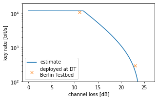
Impact of components
Laser
The system runs well with a non-tunable CW laser with 100kHz bandwidth and center wavelength at around 1550nm.
The allowed center wavelength depends on the components chosen: the beam splitters in the interferometer, optical filter, modulators. We tested the system between 1530nm and 1570nm. The qber went up slightly from 4% at 1550nm to 6% at 1530nm and 1565nm.
The bandwidth of the laser must be small enough to interfere with high visility on the unbalanced Mach-Zehnder interferometer. We can roughly estimate the qber contribution as \( 1 - \exp(-\tau/\tau_c) \), where \( \tau_c \) is the coherence time and \( \tau \) the delay of the Mach-Zehnder.
The stability of the laser must be good enough to allow phase stabilization of the Mach-Zehnder interferometer (which is done based on SPD counts, which is slow). As a rule of thumb, a pi phasedrift of the Mach-Zehnder interferometer should be of the order of 1s or slower. This is fine for thermal drifts. However, if the laser is tunable, it will often actively tune the center wavelength. We tested two tunable lasers. Only one of them worked in it's ultra-narrow linewidth mode: The RIO COLORADO Widely Tunable 1550nm Narrow Linewidth Laser Source.
Detector
The detector is a crutial component of the system because it directly influences the key rate through the maximimum click rate, maximum gate rate (repetition rate) and it's contribution to the qber from dark counts and afterpulses.
We use the Aurea OEM module in gated mode. Additionally we apply software filters around the peaks to reduce background as much as possible. We set the dead time to around 20us. Interestingly, we noticed that changing the detection efficiency setting between 10% and 20% yield similar key rates. Even though the count rates are higher at a higher detection efficiency, the qber also goes up and/or the dead time needs to be increased.